
herunterladen
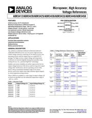
Micropower, High Accuracy
Voltage References
ADR3412/ADR3420/ADR3425/ADR3430/ADR3433/ADR3440/ADR3450
Rev. B
Information furnished by Analog Devices is believed to be accurate and reliable. However, no
responsibility is assumed by Analog Devices for its use, nor for any infringements of patents or other
rights of third parties that may result from its use. Specifications subject to change without notice. No
license is granted by implication or otherwise under any patent or patent rights of Analog Devices.
Trademarks and registered trademarks are the property of their respective owners.
One Technology Way, P.O. Box 9106, Norwood, MA 02062-9106, U.S.A.
Tel: 781.329.4700 www.analog.com
Fax: 781.461.3113 ©2010 Analog Devices, Inc. All rights reserved.
FEATURES
Initial accuracy: ±0.1% (maximum)
Maximum temperature coefficient: 8 ppm/°C
Operating temperature range: −40°C to +125°C
Output current: +10 mA source/−3 mA sink
Low quiescent current: 100 μA (maximum)
Low dropout voltage: 250 mV at 2 mA
Output noise (0.1 Hz to 10 Hz): <10 μV p-p at 1.2 V (typical)
6-lead SOT-23
APPLICATIONS
Precision data acquisition systems
Industrial instrumentation
Medical devices
Battery-powered devices
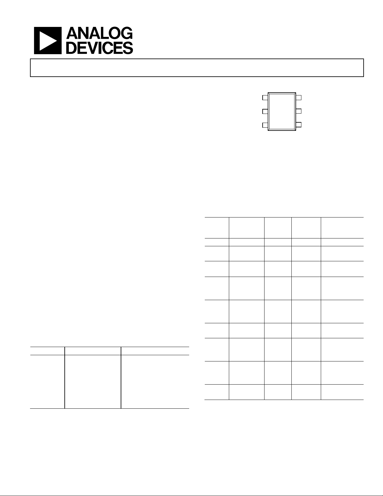
PIN CONFIGURATION
GND FORCE
1
GND SENSE
2
ENABLE
3
V
OUT
FORCE
6
V
OUT
SENSE
5
V
IN
4
ADR34xx
TOP VIEW
(Not to Scale)
08440-001
Figure 1. 6-Lead SOT-23
GENERAL DESCRIPTION
The ADR3412/ADR3420/ADR3425/ADR3430/ADR3433/
ADR3440/ADR3450 are low cost, low power, high precision
CMOS voltage references, featuring ±0.1% initial accuracy, low
operating current, and low output noise in a small SOT-23
package. For high accuracy, output voltage and temperature
coefficient are trimmed digitally during final assembly using
Analog Devices, Inc., patented DigiTrim® technology.
Stability and system reliability are further improved by the low
output voltage hysteresis of the device and low long-term output
voltage drift. Furthermore, the low operating current of the
device (100 μA maximum) facilitates usage in low power
devices, and its low output noise helps maintain signal integrity
in critical signal processing systems.
These CMOS are available in a wide range of output voltages, all
of which are specified over the industrial temperature range of
−40°C to +125°C.
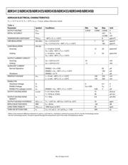
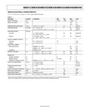
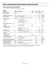
Table 1. Selection Guide
Model Output Voltage (V) Input Voltage Range (V)
ADR3412 1.200 2.3 to 5.5
ADR3420 2.048 2.3 to 5.5
ADR3425 2.500 2.7 to 5.5
ADR3430 3.000 3.2 to 5.5
ADR3433 3.300 3.5 to 5.5
ADR3440 4.096 4.3 to 5.5
ADR3450 5.000 5.2 to 5.5
Table 2. Voltage Reference Choices from Analog Devices
V
OUT
(V)
Low Cost/
Low Power
Ultralow
Power
Low
Noise
High Voltage,
High Perfor-
mance
0.5/1.0 ADR130
1.2 ADR3412
ADR280
2.048 ADR360 REF191 ADR430
ADR3420 ADR440
2.5 ADR3425 ADR291 ADR431 ADR03
AD1582 REF192 ADR441 AD780
ADR361
3.0 ADR3430 REF193 ADR433 ADR06
AD1583
ADR363 ADR443 AD780
3.3 ADR366
ADR3433
REF196
4.096 ADR3440 ADR292 ADR434
AD1584
ADR364 REF198 ADR444
5.0 ADR3450 ADR293 ADR435 ADR02
AD1585 REF195 ADR445
ADR365 AD586
10.0 ADR01
AD587
Verzeichnis
- ・ Konfiguration des Pinbelegungsdiagramms on Seite 1 Seite 11
- ・ Abmessungen des Paketumrisses on Seite 22
- ・ Teilenummerierungssystem on Seite 22
- ・ Blockdiagramm on Seite 19
- ・ Beschreibung der Funktionen on Seite 1 Seite 11
- ・ Technische Daten on Seite 1 Seite 3 Seite 10
- ・ Anwendungsbereich on Seite 1 Seite 11 Seite 20 Seite 21
- ・ Elektrische Spezifikation on Seite 3 Seite 4 Seite 5 Seite 6 Seite 7