
herunterladen
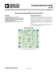
Evaluation Board User Guide
UG-186
One Technology Way • P. O. Box 9106 • Norwood, MA 02062-9106, U.S.A. • Te l: 781.329.4700 • Fax: 781.461.3113 • www.analog.com
User Guide for ADP322/ADP323 Evaluation Board
PLEASE SEE THE LAST PAGE FOR AN IMPORTANT
WARNING AND LEGAL TERMS AND CONDITIONS.
Rev. 0 | Page 1 of 12
FEATURES
Bias voltage range (V
BIAS
): 2.5 V to 5.5 V
LDO input voltage range (V
IN1
/V
IN2
, V
IN3
): 1.8 V to 5.5 V
Output current range: 0 mA to 200 mA per output
Output voltage accuracy: ±1%
Operating temperature range: −40°C to +125°C
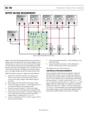
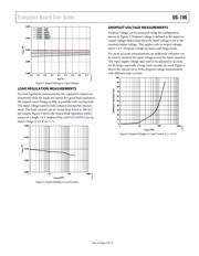
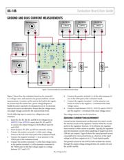
GENERAL DESCRIPTION
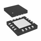
The ADP322/ADP323 evaluation board is used to demonstrate the
functionality of the ADP322/ADP323 series of linear regulators.
Simple device measurements, such as line and load regulation,
dropout voltage, and ground current, can be demonstrated with
two voltage supplies, a few voltmeters, current meters, and load
resistors.
For more details about the ADP322/ADP323 linear regulators,
see the ADP322/ADP323 data sheet.
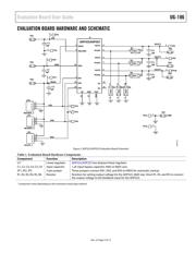
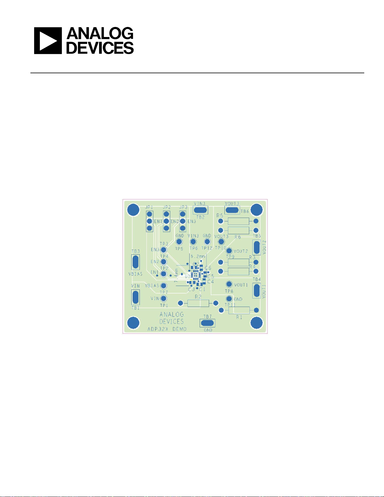
EVALUATION BOARD
0
9299-001
Figure 1. ADP322/ADP323 Evaluation Board
Verzeichnis