
herunterladen
Micro PMU with 800 mA Buck, 300 mA LDO,
Supervisory, Watchdog, and Manual Reset
Data Sheet
ADP5043
Rev. A
Information furnished by Analog Devices is believed to be accurate and reliable. However, no
responsibility is assumed by Analog Devices for its use, nor for any infringements of patents or other
rights of third parties that may result from its use. Specifications subject to change without notice. No
license is granted by implication or otherwise under any patent or patent rights of Analog Devices.
Trademarks and registered trademarks are the property of their respective owners.
One Technology Way, P.O. Box 9106, Norwood, MA 02062-9106, U.S.A.
Tel: 781.329.4700 www.analog.com
Fax: 781.461.3113 ©2011 Analog Devices, Inc. All rights reserved.
FEATURES
Input voltage range: 2.3 V to 5.5 V
One 800 mA buck regulator
One 300 mA LDO
20-lead, 4 mm × 4 mm LFCSP package
Initial regulator accuracy: ±1%
Overcurrent and thermal protection
Soft start
Undervoltage lockout
Open-drain processor reset with threshold monitoring
±1.5% threshold accuracy over the full temperate range
Guaranteed reset output valid to V
CC
= 1 V
Dual watchdog for secure systems
Watchdog 1 controls reset
Watchdog 2 controls reset and regulators power cycle
Buck regulator key specifications
Current-mode topology for excellent transient response
3 MHz operating frequency
Uses tiny multilayer inductors and capacitors
Mode pin selects forced PWM or auto PFM/PSM modes
100% duty cycle low dropout mode
LDO key specifications
Low V
IN
from 1.7 V to 5.5 V
Stable with1 µF ceramic output capacitors
High PSRR, 60 dB up to 1 kHz/10 kHz
Low output noise
Low dropout voltage: 150 mV at 300 mA load
−40°C to +125°C junction temperature range
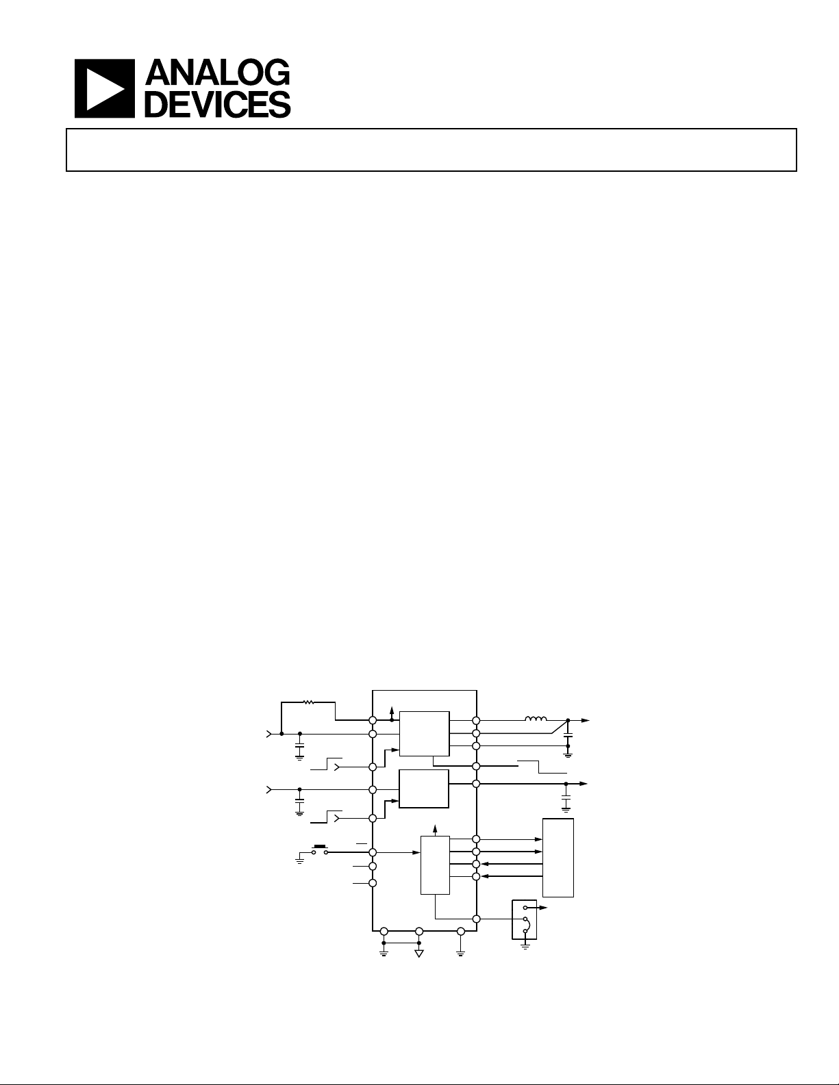
GENERAL DESCRIPTION
The ADP5043 combines one high performance buck regulator
and one low dropout regulator (LDO) in a small 20-lead LFCSP
to meet demanding performance and board space requirements.
The high switching frequency of the buck regulator enables use
of tiny multilayer external components and minimizes board space.
The MODE pin selects the buck’s mode of operation. When set
to logic high, the buck regulator operates in forced PWM mode.
When the MODE pin is set to logic low, the buck regulator
operates in PWM mode when the load is around the nominal
value. When the load current falls below a predefined threshold,
the regulator operates in power save mode (PSM) improving
the light-load efficiency.
The low quiescent current, low dropout voltage, and wide input
voltage range of the ADP5043 LDO extend the battery life of
portable devices. The LDO maintains a power supply rejection
of greater than 60 dB for frequencies as high as 10 kHz while
operating with a low headroom voltage.
Each regulator is activated by a high level on the respective
enable pin. The ADP5043 is available with factory programmable
default output voltages and can be set to a wide range of options.
The ADP5043 contains supervisory circuits that monitor
power supply voltage levels and code execution integrity in
microprocessor-based systems. The ADP5043 also provides
power-on reset signals. An on-chip dual watchdog timer can
reset the microprocessor or power cycle the system (Watchdog 2)
if it fails to strobe within a preset timeout period.
HIGH LEVEL BLOCK DIAGRAM
VIN
WD1 MODE
SELECTION
FPWM
PSM/PWM
MODE
SW
VOUT1
PGND
C6
10µF
L1
1µH
EN_BK
BUCK
EN_LDO
LDO
VIN1
EN1
VIN2
EN2
C2
1µF
VOUT2
GND GND
C5
4.7µF
ON
OFF
ON
OFF
NC
VIN1 = 2.3V
TO 5.5V
AVIN
R
FILT
30Ω
VIN2 = 1.7V
TO 5.5V
MR
C1
1µF
MICROPROCESSOR
SUPERVISOR
WSTAT
WMOD
WDI1
WDI2
nRSTO
NC
AGND
AVIN
AVIN
ADP5043
V
OUT1
@
800mA
V
OUT2
@
300mA
09682-001
Figure 1.
Verzeichnis
- ・ Konfiguration des Pinbelegungsdiagramms on Seite 8 Seite 30
- ・ Abmessungen des Paketumrisses on Seite 30
- ・ Teilenummerierungssystem on Seite 30
- ・ Blockdiagramm on Seite 1 Seite 16 Seite 27
- ・ Typisches Anwendungsschaltbild on Seite 21
- ・ Schweißen Temperatur on Seite 7
- ・ Beschreibung der Funktionen on Seite 1 Seite 8 Seite 30
- ・ Technische Daten on Seite 1 Seite 3 Seite 5 Seite 6 Seite 7
- ・ Anwendungsbereich on Seite 21
- ・ Elektrische Spezifikation on Seite 9