
herunterladen

ADP1829, APD210X and ADP171X
Reference Design
Preliminary Technical Data
FCDC 00057
Rev. A
Reference designs are as supplied “as is” and without warranties of any kind, express,
implied, or statutory including, but not limited to, any implied warranty of
merchantability or fitness for a particular purpose. No license is granted by implication or
otherwise under any patents or other intellectual property by application or use of
reference designs. Information furnished by Analog Devices is believed to be accurate and
reliable. However, no responsibility is assumed by Analog Devices for its use, nor for any
infringements of patents or other rights of third parties that may result from its use.
Analog Devices reserves the right to change devices or specifications at any time without
notice. Trademarks and registered trademarks are the property of their respective
owners. Reference designs are not authorized to be used in life support devices or
systems.
One Technology Way, P.O. Box 9106, Norwood, MA 02062-9106,
U.S.A.
Tel: 781.329.4700
www.analo
g
Fax: 781.461.3113 ©2007 Analog Devices, Inc. All rights res
e
FEATURES
Seven Output Voltages: 5.0 V, 3.6 V, 3.3 V, 2.5 V, 1.8 V, 1.2 V, 0.9 V
Output Current: 0.002 A to 3.0 A
Input voltage: 10.8-13.2 V
Ripple 2% ppk of Output Voltage
Transient step ±5%, 50% max load
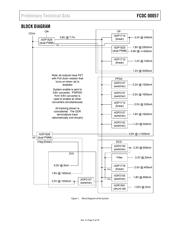
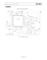
ADP1829, APD210X AND ADP171X REFERENCE DESIGN DESCRIPTION
This ADP1829, APD210X and ADP171X Reference Design uses 10.8 V to 13.2 V for the input voltage. The output voltages
and currents are as follows:
• V
OUT1
= 3.6 V with a maximum output current of 7.7 A for intermediate rail,
• V
OUT2
= 1.2 V with a maximum output current of 3.0 A for VP,
• V
OUT3
= 1.8 V with a maximum output current of 2.8 A for VP,
• V
OUT4
= 0.9 V with a maximum output current of +/-0.5 A for VP,
• V
OUT5
= 3.3 V with a maximum output current of 0.34 A for VP,
• V
OUT6
= 1.2 V with a maximum output current of 0.1 A for VP,
• V
OUT7
= 3.3 V with a maximum output current of 1.5 A for FPGA,
• V
OUT8
= 2.5 V with a maximum output current of 1.6 A for FPGA,
• V
OUT9
= 1.8 V with a maximum output current of 1.6 A for FPGA,
• V
OUT10
= 1.2 V with a maximum output current of 0.5 A for FPGA,
• V
OUT11
= 2.5 V with a maximum output current of 0.3 A for FPGA,
• V
OUT12
= 1.8 V with a maximum output current of 1.95 A for DVI,
• V
OUT13
= 0.9 V with a maximum output current of +/-0.5 A for FPGA,
• V
OUT14
= 3.3 V with a maximum output current of 1.55 A for DVI,
• V
OUT15
= 5.0 V with a maximum output current of 0.005 A for DVI,
• V
OUT16
= 3.3 V with a maximum output current of 0.6 A for DCD,
• V
OUT17
= 1.8 V with a maximum output current of 0.9 A for DCD,
• V
OUT18
= 3.3 V with a maximum output current of 0.02 A for DCD,
• V
OUT19
= 2.5 V with a maximum output current of 0.4 A for DCD,
• V
OUT20
= 1.25 V with a maximum output current of 0.002 A for DCD,
Verzeichnis