
herunterladen
Evaluation Board User Guide
UG-208
One Technology Way • P. O. Box 9106 • Norwood, MA 02062-9106, U.S.A. • Te l: 781.329.4700 • Fax: 781.461.3113 • www.analog.com
1 GSPS Quadrature Digital Upconverter with 14-Bit DAC Evaluation Board
PLEASE SEE THE LAST PAGE FOR AN IMPORTANT
WARNING AND LEGAL TERMS AND CONDITIONS.
Rev. A | Page 1 of 32
FEATURES
1 GSPS internal clock speed (up to 400 MHz analog output)
Integrated 1 GSPS 14-bit DAC
250 MHz I/Q data throughput rate
Phase noise ≤ −125 dBc/Hz (400 MHz carrier @ 1 kHz offset)
Excellent dynamic performance >80 dB narrow-band SFDR
8 programmable profiles for shift keying
Sin(x)/(x) correction (inverse sinc filter)
Reference clock multiplier
Internal oscillator for a single crystal operation
Software and hardware controlled power-down
Integrated RAM
Phase modulation capability
Multichip synchronization
Easy interface to Blackfin SPORT
Interpolation factors from 4× to 252×
Interpolation DAC mode
Gain control DAC
Internal divider allows references up to 2 GHz
1.8 V and 3.3 V power supplies
100-lead TQFP_EP package
PACKAGE CONTENTS
AD9957 evaluation board
AD9957/PCB installation software
USB cable
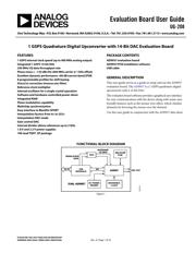
GENERAL DESCRIPTION
This user guide serves as a guide to setup and use the AD9957
evaluation board. The AD9957 is a 1 GSPS quadrature digital
upconverter with a 14-bit DAC.
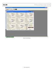
The evaluation board software provides a graphical user interface
for easy communication with the device along with many user-
friendly features such as the mouse-over effect, which clarifies
elements by hovering the mouse over the element.
Use this user guide in conjunction with the AD9957 data sheet.
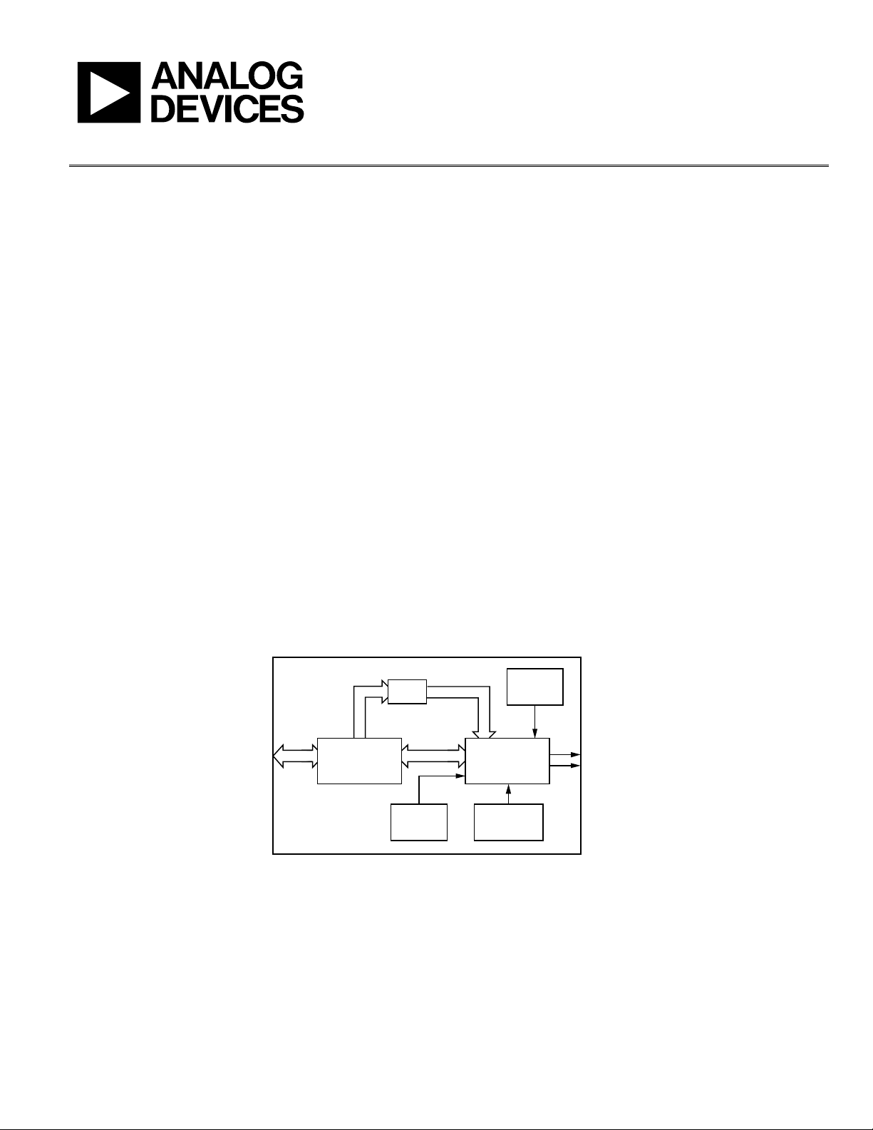
FUNCTIONAL BLOCK DIAGRAM
AD9957
SPI
FIFO
MULTICHIP
SYNC
DC POWER
HEADER
REFERENCE
CLOCK
BASEBAND
I/Q DATA
TO PC
DAC OUT
07801-001
EVAL-AD9957
USB
INTERFACE
MODULATION
DATA
Figure 1.