
herunterladen
AD9889B Hardware User’s Guide 6/7/2007
HARDWARE FEATURES
• 3 packages (80 pin LQFP, 64 pin LFCSP, 76 Ball
BGA)
• Extended temperature range (LFCSP, BGA)
• Operation up to 165MHz
• INT output pin eliminates constant I2C monitoring
• AD9889B only requires 1.8V supply
• AD9889B accepts 1.8V or 3.3V input levels
• AD9889B accepts several video input formats
• Supports I2S & SPDIF audio input format
• No audio Master clock required for I2S & SPDIF
• On Chip CPU performs HDCP & EDID operations
INTRODUCTION
The AD9889B is a high speed HDMI transmitter which
operates up to 165MHz (UXGA 60Hz). Careful Hardware
design (schematics and PCB layout) is recommended to
optimize the AD9889B’s performance and to ensure HDMI
compliance.
The AD9889B Hardware User’s Guide (HUG) provides
guidelines to design the schematics and board layout for the
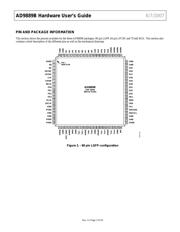
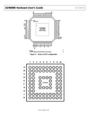
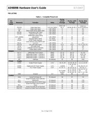
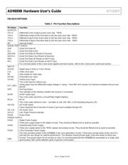
AD9889B implementation. Section 3 (“pin out & mechanical
drawings”) contains information about the three available
packages: 80 pin LQFP, 64 pin LFCSP, and 76 ball BGA.
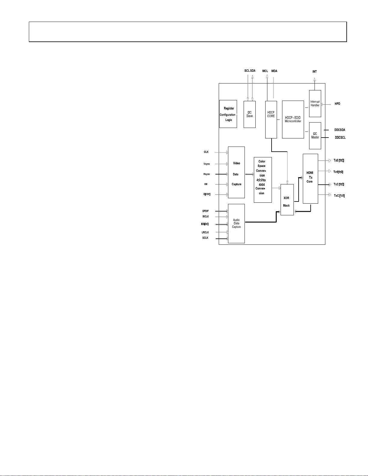
Section 4 is an overview of the AD9889B’s functional blocks
(including a brief description for each block) to provide an
understanding of the AD9889B’s functional and performance
capabilities.
Section 5 lists the many input video and audio formats
supported by the AD9889B, and explains how to connect
these signals to the AD9889B’s inputs. Section 6 has the
relevant information about the AD9889B’s outputs: TMDS,
DDC lines, INT, and Master I2C lines for HDCP. Sections 7
and 8 cover the power supply and current reference
connections.
Sections 5 through 8 of the Hardware User’s Guide also
contains recommendations (such as external component
value and layout design guidelines) to optimize the
AD9889B’s performance and to ensure HDMI compliance.
Section 9 contains the schematics of a typical AD9889B
hardware implementation. Finally section 10 is a reference
documents list. The AD9889B Software User’s Guide and a
Driver’s User Guide are also available.
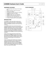
BLOCK DIAGRAM
Figure 1. - Functional Block Diagram
SUPPORTED INPUT FORMATS
• 24 bit RGB 444 (separate syncs)
• 24 bit YCbCr 444 (separate syncs)
• 16, 20, 24 bit YCbCr 422 (embedded or separate
syncs)
• 8, 10, 12 bit YCbCr 422 (2x pixel clock with
embedded or separate syncs)
• 8, 10, 12 bit YCbCr 422 (DDR with separate syncs)
• 12 bit RGB 444 (DDR with separate syncs)
• 12 bit YCbCr 444 (DDR with separate syncs)
SUPPORTED OUTPUT FORMATS:
• 24 bit RGB 4:4:4
• 24 bit YCbCr 4:4:4
• 16 bit YCbCr 4:2:2
• 20 bit YCbCr 4:2:2
• 24 bit YCbCr 4:2:2
FORMAT STANDARDS
In this document, ADI has chosen to represent data in the following ways:
0xNN Hexadecimal ( base-16 )numbers are represented using the ‘C’ language notation, preceded by ‘0x’.
0bNN Binary (base-2) numbers are represented using ‘C’ language notation, preceded by ‘0b’.
NN Decimal (base-10) numbers are represented using no additional prefixes or suffixes.
Bit Bits are numbered in little-endian format, i.e. the least-significant bit of a byte or word is referred to as bit 0.
Verzeichnis