
herunterladen
AN-957
APPLICATION NOTE
One Technology Way • P. O. Box 9106 • Norwood, MA 02062-9106, U.S.A. • Te l: 781.329.4700 • Fax: 781.461.3113 • www.analog.com
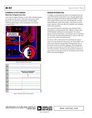
Layout Guidelines for the AD7147 and AD7148 CapTouch Controllers
by Susan Pratt
Rev. 0 | Page 1 of 4
INTRODUCTION
This application note gives layout guidelines to assist with
designing sensors for the AD7147 and AD7148 CapTouch™
controllers, covers sensor construction and PCB stack-up,
gives general-purpose layout guidelines, offers guidelines
for EMI and ESD sensitive designs, and proposes tips on
integrating the sensors into final designs.
The AD7147 and AD7148 are capacitive-to-digital converters
(CDCs) for single electrode sensors. The AD7147 is a 13 capa-
citive input device, while the AD7148 is an 8 input device.
The AD7147 is designed for use with capacitance sensors
implementing functions such as buttons, scroll bars, wheels,
and touch pads. The AD7148 is for use with buttons, scroll
bars, and wheels.
SUITABLE MATERIALS FOR SENSOR
CONSTRUCTION
Any standard PCB material is suitable for capacitance sensor
design, which allows the sensors to be manufactured using
industry-standard techniques. Sensor board and trace material
examples are shown in Table 1.
Table 1. Materials Suitable for Sensor Manufacturing
Sensor Board Sensors
FR4 (and Similar) Copper
Flex (FPC or Polyamide) Copper
PET (Plastic) Indium tin oxide (ITO)/silver/carbon
Glass ITO
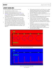
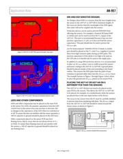
SENSOR PCB STACK-UP
The sensors should be on the top layer of the PCB. Each sensor
connects to the AD7147 or AD7148 through the CIN input
pins. Place an AC
SHIELD
plane around the sensors and sensor
traces on all layers of the PCB.
The stack-up in Table 2 is recommended to ensure there is
no cross coupling of noise onto the sensors from other signals
routed on the PCB. Use the stack-up in Table 3 only in cases
where there is sufficient space available on the PCB to ensure
no routing crosses underneath the sensors or sensor traces.
Table 2. Sensor PCB 4-Layer Stack-Up
Layer Sensors
1 (Top)
Layout sensor electrodes and CIN connection
traces; surround by 2 mm of an AC
SHIELD
plane. Place
a ground plane around board edges to protect
from ESD.
2
Place an AC
SHIELD
plane under sensors and sensor
traces (mirror AC
SHIELD
and ground plane from
Layer 1); do not place digital routing under
sensors or AC
SHIELD
.
3
Route serial interface and other signals, mirror
AC
SHIELD
and ground plane from Layer 1.
4 (Bottom)
Place the IC, serial interface, and other signal
routing here, mirror AC
SHIELD
and ground plane
from Layer 1.
Table 3. Sensor PCB 2-Layer Stack-Up
Layer Sensors
1 (Top)
Layout sensor electrodes surrounded by 2 mm of an
AC
SHIELD
plane and a ground plane around board edges
to protect from ESD.
2
Place the IC, CIN connection traces with 2 mm of an
AC
SHIELD
plane around sensor traces. Place a serial
interface, other signal routing, and other components
here surrounded by a ground plane extending to
board edges (mirror AC
SHIELD
and ground plane from
Layer 1).