
herunterladen

AN-1359
APPLICATION NOTE
One Technology Way • P. O. Box 9106 • Norwood, MA 02062-9106, U.S.A. • Tel: 781.329.4700 • Fax: 781.461.3113 • www.analog.com
Low Noise, Dual-Supply Solution Using the ADP5070 for the Precision AD5761R
Bipolar DAC in Single-Supply Systems
by Estibaliz Sanz Obaldia and James Jasper Macasaet
Rev. A | Page 1 of 16
INTRODUCTION
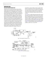
This application note describes how a system with a single
unipolar supply can be used to power components requiring
dual (bipolar) power supplies. The AD5761R, a bipolar digital-
to-analog converter (DAC), requires dual supplies to provide
bipolar output voltage ranges. The examples shown in this
application note use the ADP5070 dc-to-dc switching regulator
with the ADP7142 and ADP7182 complementary metal-oxide
semiconductor (CMOS) low dropout (LDO) linear regulators,
LC filters, and resistor dividers to generate dual supplies from a
5 V single voltage supply to power the AD5761R.
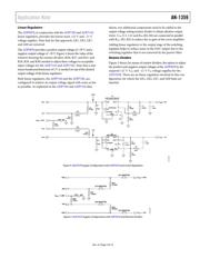
Together, the 5 V power supply and combination of the ADP5070,
ADP7142, ADP7182, and/or LC filters provide a power supply
solution for DACs that output unipolar and bipolar voltage ranges.
This solution provides noise performance similar to that of a
DAC being supplied by a dual bench power supply.
The power spectrum analysis, voltage output noise, and ac
performance data included in this application note support the
performance of this solution.
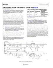
The proposed supply configurations yield different results
depending on which tests a user performs on the system. For
instance, a configuration that incorporates the ADP5070 supply
and additional LC filters is optimal for reducing the spectral
noise from 10 Hz to 10 kHz when the internal reference of the
DAC is used. An external supply, on the other hand, provides
the best result for a spectral analysis using an external reference.
Results gathered with the external supply were used as the
baseline measurement for all the supply configurations. For a
higher frequency bandwidth (10 kHz to 10 MHz), adding
CMOS LDO linear regulators to the ADP5070 supply offers the
best spectral noise performance. The resulting output spectrum
of the DAC for an LC filter and LDO configuration, which is
used to reduce the switching noise from the ADP5070, is
comparable to an external supply configuration.
The sensitivity to noise of the system determines the amount of
circuitry required to reduce the noise to acceptable levels. No
significant difference is observable between the output noise
measurements at 0.1 Hz to 10 Hz due to the inherent noise
rejection capabilities of the AD5761R. Using additional LDOs
significantly reduces the AD5761R output noise, resulting in a
performance comparable to the baseline measurement.
For the ac performance tests, the AD5761R performs within the
data sheet specifications under all presented supply configurations.
The AD5761R is a 16-bit DAC that integrates an output amplifier,
a reference buffer, and a maximum 5 ppm/°C temperature
coefficient internal reference. The AD5761R operates from a
unipolar supply of up to 30 V or a bipolar supply of −16.5 V to
0 V for V
SS
and 4.75 V to 16.5 V for V
DD
. The AD5761R offers
eight programmable output ranges, 35 nV/√Hz noise, and a
7.5 µs settling time on selected ranges.
The ADR4525, a 2.5 V voltage reference, is used across the tests
presented in this application note as an external reference to cover
applications that require ultralow noise voltage references.
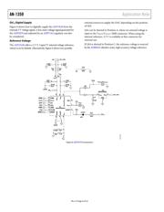
The ADP5070 is a dual, high performance, dc-to-dc regulator
that generates independently regulated positive and negative rails.
The input voltage range of 2.85 V to 15 V supports a wide variety
of applications. The integrated main switch in both regulators
enables generation of an adjustable positive output voltage up to
+39 V and a negative output voltage down to −39 V below input
voltage. The ADP5070 operates at a pin selected 1.2 MHz/2.4 MHz
switching frequency. In addition, the regulator has slew rate
control circuitry for the metal-oxide semiconductor field effect
transistor (MOSFET) driver stage to reduce electromagnetic
interference (EMI).
The ADP7142 is an LDO linear regulator that operates from 2.7 V
to 40 V and provides up to 200 mA of output current. This high
input voltage LDO linear regulator is ideal for regulating high
performance analog and mixed-signal circuits operating rails
from 40 V down to 1.2 V. Using a proprietary architecture, the
device provides high power supply rejection, low noise, and
achieves excellent line and load transient response. The ADP7142
regulator output noise is 11 μV rms at 5 V or less with the
ability to adjust the output voltage on the 5 V option to 15 V.
The ADP7182 is an LDO linear regulator that operates from
−2.7 V to −28 V and provides up to −200 mA of output current.
This high negative input voltage LDO linear regulator is ideal
for regulating high performance analog and mixed-signal
circuits operating rails from −27 V down to −1.2 V.
Verzeichnis
- ・ Blockdiagramm on Seite 3
- ・ Anwendungsbereich on Seite 3