

herunterladen
AN-1205
APPLICATION NOTE
One Technology Way • P. O. Box 9106 • Norwood, MA 02062-9106, U.S.A. • Te l: 781.329.4700 • Fax: 781.461.3113 • www.analog.com
30 V Low Cost DAC Using the AD5292 Digital Potentiometer
Rev. B | Page 1 of 3
CIRCUIT FUNCTION AND BENEFITS
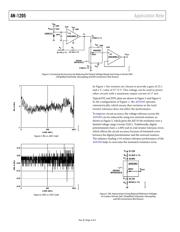
This circuit shown in Figure 1 provides a low cost, high voltage
unipolar DAC using the AD5292 digital potentiometer in
conjunction with the dual ADA4091-2 op amp and ADR512
voltage reference. This circuit offers 10-bit resolution over an
output voltage range of 0 V to 30 V and is capable of delivering
up to ±20 mA output current. The AD5292 is programmable
over an SPI-compatible serial interface.
The ±1% resistor tolerance of the AD5292 allows it to be placed
in series with external divider resistors R
3
and R
4
, as shown in
Figure 2 and Figure 5, to create a vernier DAC with 10-bit
resolution over a reduced V
OUT
range. This serves to increase
the sensitivity of the DAC, similar to adding resistance in series
with a potentiometer. In addition, the AD5292 has an internal
20-times programmable memory that allows a customized V
OUT
at power-up.
The circuit provides accurate, low noise, and low tempco output
voltage capability and is well suited for digital calibration
applications.
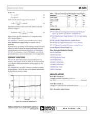
CIRCUIT DESCRIPTION
Table 1. Devices Connected/Referenced
Product Description
AD5292
Digital potentiometer, 10 bits, 1% resistor
tolerance
ADR512 Low noise, precision 1.200 V reference
ADA4091-2
Micropower, overvoltage protected (OVP)
rail-to-rail op amp
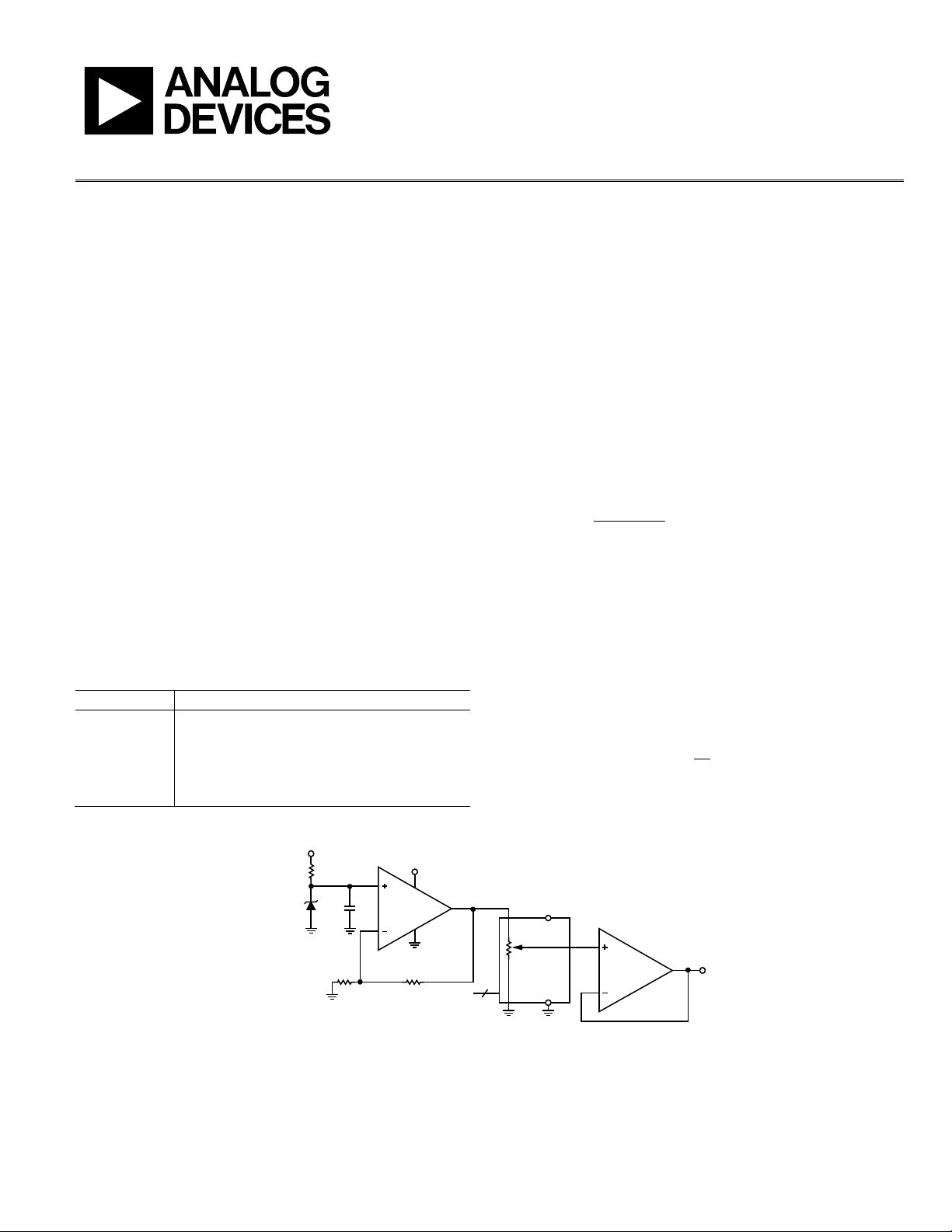
This circuit shown in Figure 1 employs the AD5292 digital
potentiometer in conjunction with the ADR512 reference and
ADA4091-2 op amp, providing a 10-bit, low cost, high voltage
DAC. The circuit guarantees monotonicity, ±1 LSB DNL, and
has an integral nonlinearity of ±2 LSB typical.
The high voltage regulator consists of a low voltage reference
followed by a noninverting amplifier whose gain is set by the
ratio of R
1
to R
2
. The ADR512 1.200 V voltage reference has
low temperature drift, high accuracy, and ultralow noise
performance.
The maximum resistor that ensures an ADR512 minimum
operating current is defined in Equation 1.
mA1
V2.1–
DD
BIAS
V
R
(1)
In Figure 1 and Figure 2 the R
BIAS
resistor is 12 kΩ, which sets
the bias current of the ADR512 at 2.4 mA.
The ADA4091-2 is an op amp that offers a low offset voltage
and rail-to-rail output. The ADR512 in combination with
the ADA4091 offer a low tempco and noise output voltage.
The resistors R
1
and R
2
adjust the gain in the amplifier. The
V
1
output voltage of U1A defines the maximum V
OUT
range
of the DAC. Equation 2 is used to calculate the resistor
values.
)1(2.1
2
1
1
R
R
V
(2)
ADA4091-2
AD5292
ADR512
V
DD
V
SS
V
DD
V
1
V
OUT
R
1
R
2
12kΩ
10nF
R
BIAS
U1A
U1B
20kΩ
1/2
ADA4091-2
2/2
+30V
+30V
V
DD
+30V
22.1kΩ ± 1%
1kΩ ± 1%
SERIAL
INTERFACE
08415-001
Figure 1. Unipolar DAC Configuration (Simplified Schematic: Decoupling and All Connections Not Shown)