
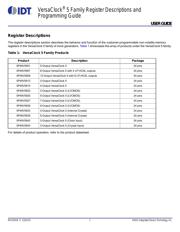
USER GUIDE
REVISION E 12/01/15 1 ©2015 Integrated Device Technology, Inc.
VersaClock
®
5 Family Register Descriptions and
Programming Guide
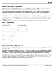
Register Descriptions
The register descriptions section describes the behavior and function of the customer-programmable non-volatile-memory
registers in the VersaClock 5 family of clock generators. Table 1 showcases the array of products under the VersaClock 5 family.
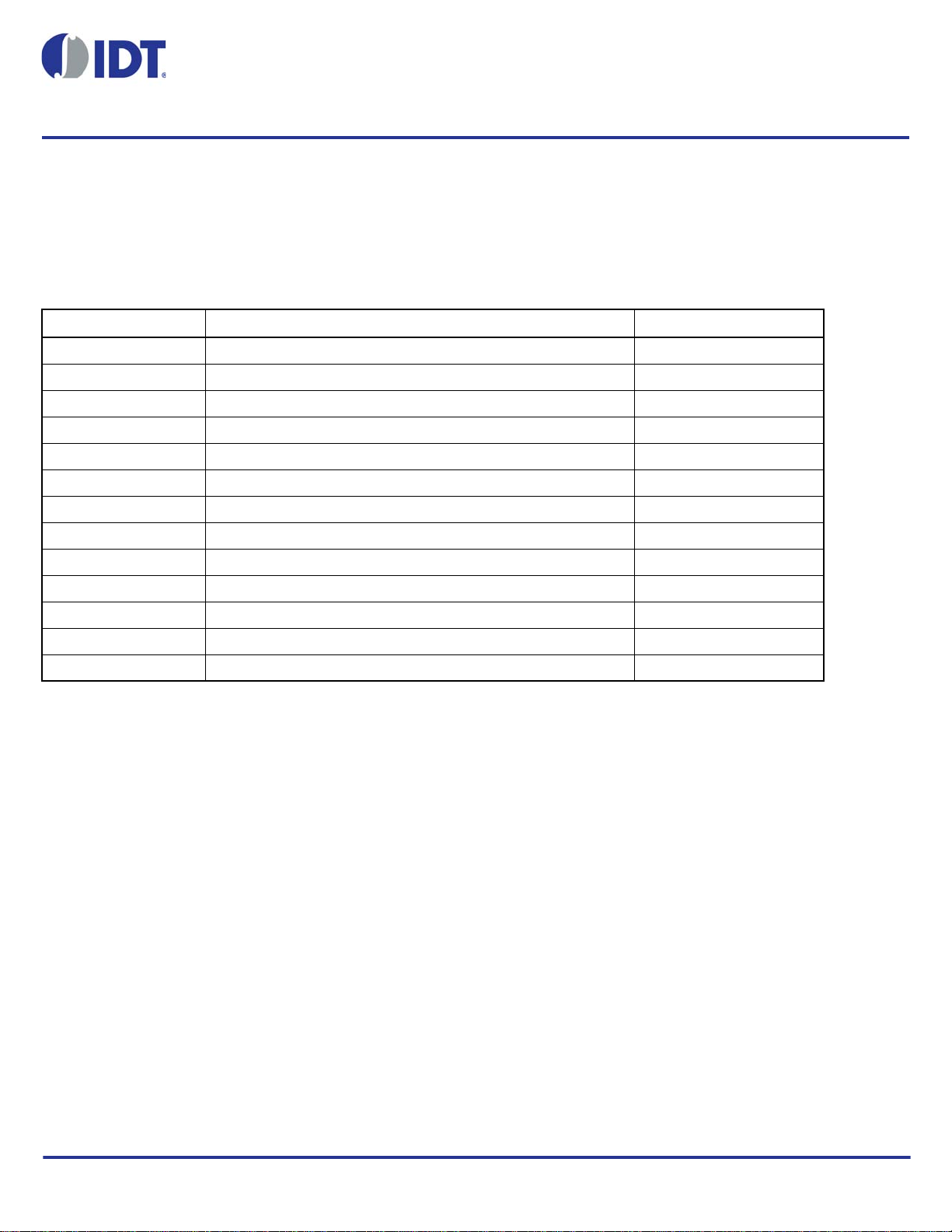
Table 1: VersaClock 5 Family Products
For details of product operation, refer to the product datasheet.
Product Description Package
5P49V5901 5-Output VersaClock 5 24 pins
5P49V5907 8-Output VersaClock 5 with 4 LP-HCSL outputs 40 pins
5P49V5908 12-Output VersaClock 5 with 8 LP-HCSL outputs 40 pins
5P49V5913 3-Output VersaClock 5 24 pins
5P49V5914 4-Output VersaClock 5 24 pins
5P49V5923 3-Output VersaClock 5 (LVCMOS) 24 pins
5P49V5925 5-Output VersaClock 5 (LVCMOS) 24 pins
5P49V5927 7-Output VersaClock 5 (LVCMOS) 24 pins
5P49V5929 9-Output VersaClock 5 (LVCMOS) 24 pins
5P49V5933 3-Output VersaClock 5 (Internal Crystal) 24 pins
5P49V5935 5-Output VersaClock 5 (Internal Crystal) 24 pins
5P49V5943 3-Output VersaClock 5 (Clock Input) 24 pins
5P49V5944 3-Output VersaClock 5 (Crystal Input) 24 pins
Verzeichnis