
herunterladen
© Semiconductor Components Industries, LLC, 2009
June, 2009 − Rev. 3
1 Publication Order Number:
Z0103MN/D
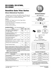
Z0103MN, Z0107MN,
Z0109MN
Sensitive Gate Triac Series
Silicon Bidirectional Thyristors
Designed for use in solid state relays, MPU interface, TTL logic and
other light industrial or consumer applications. Supplied in surface
mount package for use in automated manufacturing.
Features
• Sensitive Gate Trigger Current in Four Trigger Modes
• Blocking Voltage to 600 V
• Glass Passivated Surface for Reliability and Uniformity
• Surface Mount Package
• These are Pb−Free Devices
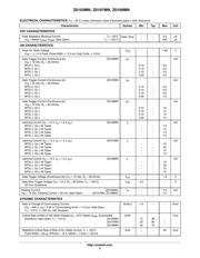
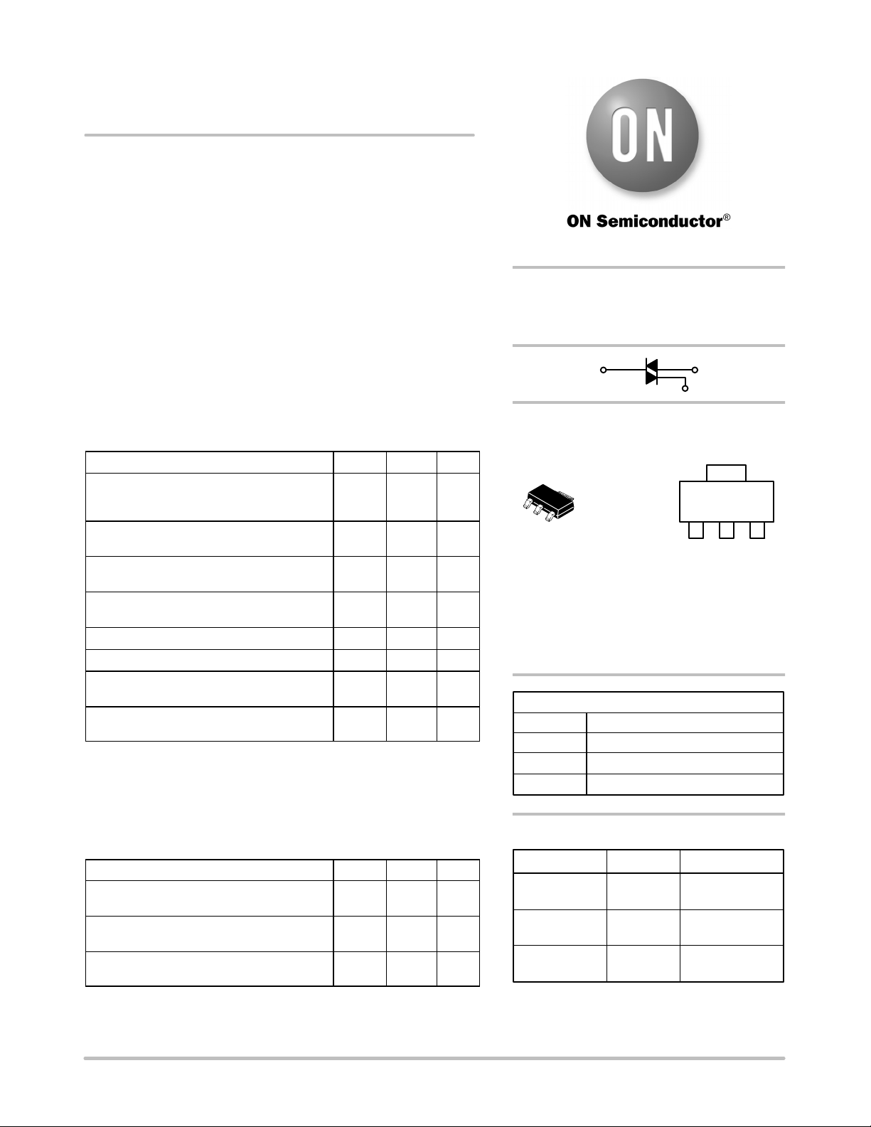
MAXIMUM RATINGS (T
J
= 25°C unless otherwise noted)
Rating Symbol Value Unit
Peak Repetitive Off−State Voltage (Note 1)
(Sine Wave, 50 to 60 Hz, Gate Open,
T
J
= −40 to +125°C)
V
DRM,
V
RRM
600 V
On−State Current RMS (T
C
= 80°C)
(Full Sine Wave 50 to 60 Hz)
I
T(RMS)
1.0 A
Peak Non−repetitive Surge Current (One Full
Cycle Sine Wave, 60 Hz, T
C
= 25°C)
I
TSM
8.0 A
Circuit Fusing Considerations
(Pulse Width = 8.3 ms)
I
2
t 0.4 A
2
s
Average Gate Power (T
C
= 80°C, t v 8.3 ms) P
G(AV)
1.0 W
Peak Gate Current (t v 20 ms, T
J
= +125°C)
I
GM
1.0 A
Operating Junction Temperature Range T
J
−40 to
+125
°C
Storage Temperature Range T
stg
−40 to
+150
°C
Stresses exceeding Maximum Ratings may damage the device. Maximum
Ratings are stress ratings only. Functional operation above the Recommended
Operating Conditions is not implied. Extended exposure to stresses above the
Recommended Operating Conditions may affect device reliability.
1. V
DRM
and V
RRM
for all types can be applied on a continuous basis. Blocking
voltages shall not be tested with a constant current source such that the
voltage ratings of the devices are exceeded.
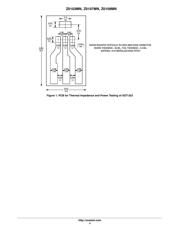
THERMAL CHARACTERISTICS
Characteristic Symbol Max Unit
Thermal Resistance, Junction−to−Ambient PCB
Mounted per Figure 1
R
q
JA
156 °C/W
Thermal Resistance, Junction−to−Tab Meas-
ured on MT2 Tab Adjacent to Epoxy
R
q
JT
25 °C/W
Maximum Device Temperature for
Soldering Purposes for 10 Secs Maximum
T
L
260 °C
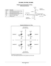
TRIAC
1.0 AMPERE RMS
600 VOLTS
MT1
G
MT2
4
23
PIN ASSIGNMENT
1
2
3 Gate
Main Terminal 1
Main Terminal 2
4
Main Terminal 2
http://onsemi.com
SOT−223
CASE 318E
STYLE 11
MARKING
DIAGRAM
AYW
10XMN G
G
A = Assembly Location
Y = Year
W = Work Week
10XMN = Device Code
x = 3, 7, 9
G = Pb−Free Package
(Note: Microdot may be in either location)
1
Device Package Shipping
†
ORDERING INFORMATION
†For information on tape and reel specifications,
including part orientation and tape sizes, please
refer to our Tape and Reel Packaging Specification
Brochure, BRD8011/D.
Z0103MNT1G SOT−223
(Pb−Free)
1000/Tape & Reel
Z0107MNT1G SOT−223
(Pb−Free)
1000/Tape & Reel
Z0109MNT1G SOT−223
(Pb−Free)
1000/Tape & Reel
Verzeichnis