
herunterladen
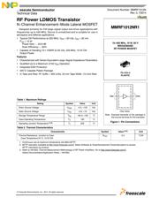
MMRF1012NR1
1
RF Device Data
Freescale Semiconductor, Inc.
RF Power LDMOS Transistor
N--Channel Enhancement--Mode Lateral MOSFET
Designed primarily for CW large--signal output and driver applications with
frequencies up to 450 MHz. Device is unmatched and is suitable for use in
aerospace and defense applications.
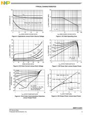
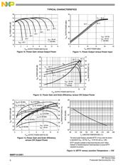
Typical CW Performance at 220 MHz: V
DD
=50Vdc,I
DQ
=30mA,
P
out
=10W
Power Gain — 23.9 dB
Drain Efficiency — 62%
Capable of Handling 10:1 VSWR @ 50 Vdc, 220 MHz, 10 W CW
Output Power
Features
Characterized with Series Equivalent Large--Signal Impedance Parameters
Qualified Up to a Maximum of 50 V
DD
Operation
Integrated ESD Protection
225C Capable Plastic Package
In Tape and Reel. R1 Suffix = 500 Units, 24 mm Tape Width, 13--inch Reel.
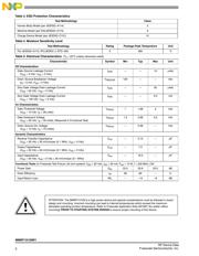
Table 1. Maximum Ratings
Rating Symbol Value Unit
Drain--Source Voltage V
DSS
--0.5, +120 Vdc
Gate--Source Voltage V
GS
--0.5, +10 Vdc
Storage Temperature Range T
stg
-- 65 to +150 C
Case Operating Temperature T
C
150 C
Operating Junction Temperature
(1,2)
T
J
225 C
Table 2. Thermal Characteristics
Characteristic Symbol Value
(2,3)
Unit
Thermal Resistance, Junction to Case
Case Temperature 81C, 10 W CW
R
JC
3.0 C/W
1. Continuous use at maximum temperature will affect MTTF.
2. MTTF calculator available at http://www.freescale.com/rf
. Select Software & Tools/Development Tools/Calculators to access
MTTF calculators by product.
3. Refer to AN1955, Thermal Measurement Methodology of RF Power Amplifiers. Go to http://www.freescale.com/rf
.
Select Documentation/Application Notes -- AN1955.
Document Number: MMRF1012N
Rev. 0, 7/2014
Freescale Semiconductor
Technical Data
10--450 MHz, 10 W, 50 V
BROADBAND
RF POWER MOSFET
MMRF1012NR1
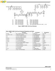
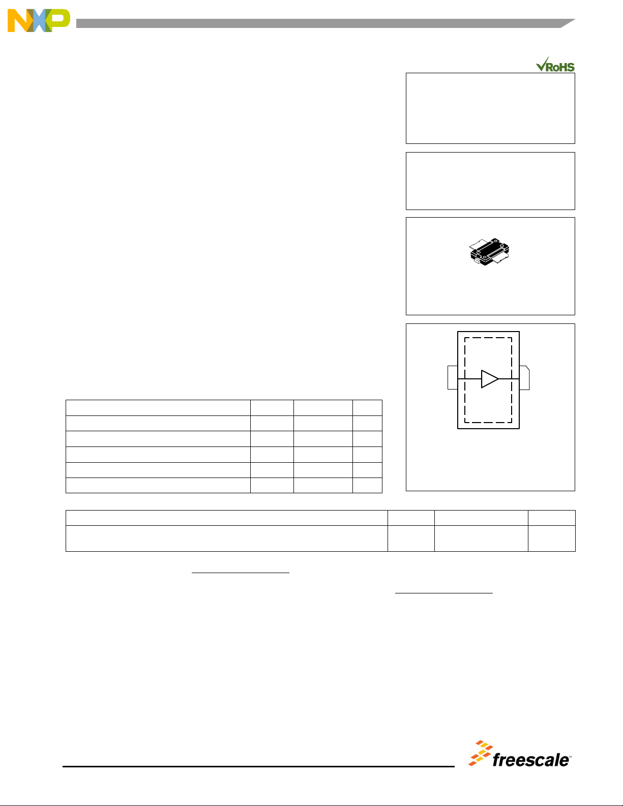
T O -- 2 7 0 -- 2
PLASTIC
Note: Exposed backside of the package is
the source terminal for the transistor.
(Top View)
Drain
21
Figure 1. Pin Connections
Gate
Freescale Semiconductor , Inc., 2014.
A
ll rights reserved.
Verzeichnis