

herunterladen
0
0.2
0.4
0.6
0.8
1
1.2
1.4
1.6
1.8
2
2.2
2.4
2.6
2.8
3
3.2
3.4
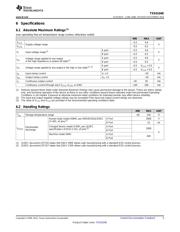
0 1 2 3 4 5
Output Voltage (V)
Input Voltage (V)
VGATE = 4.3 V
VGATE = 3.5 V
VGATE = 2.8 V
VGATE = 2.5 V
VGATE = 2.2 V
C001
V
GATE
= 4.3 V
V
GATE
= 3.5 V
V
GATE
= 2.8 V
V
GATE
= 2.5 V
V
GATE
= 2.2 V
Product
Folder
Sample &
Buy
Technical
Documents
Tools &
Software
Support &
Community
Reference
Design
TXS0104E
SCES651F –JUNE 2006–REVISED DECEMBER 2014
TXS0104E 4-Bit Bidirectional Voltage-Level Translator For Open-Drain and Push-Pull
Applications
1 Features 3 Description
This 4-bit non-inverting translator uses two separate
1
• No Direction-Control Signal Needed
configurable power-supply rails. The A port is
• Max Data Rates
designed to track V
CCA
. V
CCA
accepts any supply
– 24 Mbps (Push Pull)
voltage from 1.65 V to 3.6 V. V
CCA
must be less than
or equal to V
CCB
. The B port is designed to track
– 2 Mbps (Open Drain)
V
CCB
. V
CCB
accepts any supply voltage from 2.3 V to
• Available in the Texas Instruments NanoFree™
5.5 V. This allows for low-voltage bidirectional
Package
translation between any of the 1.8-V, 2.5-V, 3.3-V,
• 1.65 V to 3.6 V on A port and 2.3 V to 5.5 V on B
and 5-V voltage nodes.
port (V
CCA
≤ V
CCB
)
When the output-enable (OE) input is low, all outputs
• No Power-Supply Sequencing Required – V
CCA
or
are placed in the high-impedance state.
V
CCB
Can Be Ramped First
The TXS0104E is designed so that the OE input
• Latch-Up Performance Exceeds 100 mA Per
circuit is supplied by V
CCA
.
JESD 78, Class II
To ensure the high-impedance state during power up
• ESD Protection Exceeds JESD 22
or power down, OE should be tied to GND through a
– A Port
pulldown resistor; the minimum value of the resistor is
determined by the current-sourcing capability of the
– 2000-V Human-Body Model (A114-B)
driver.
– 200-V Machine Model (A115-A)
– 1000-V Charged-Device Model (C101)
Device Information
(1)
– B Port
PART NUMBER PACKAGE BODY SIZE (NOM)
– 15-kV Human-Body Model (A114-B)
SOIC (14) 8.65 mm × 3.91 mm
– 200-V Machine Model (A115-A)
TSSOP (14) 5.00 mm × 4.40 mm
TXS0104E BGA (12) 2.00 mm × 2.50 mm
– 1000-V Charged-Device Model (C101)
VQFN (14) 3.50 mm × 3.50 mm
• IEC 61000-4-2 ESD (B Port)
DSBGA (12) 1.90 mm × 1.90 mm
– ±8-kV Contact Discharge
(1) For all available packages, see the orderable addendum at
– ±10-kV Air-Gap Discharge
the end of the datasheet.
2 Applications
Transfer Characteristics of an N-Channel
Transistor
• Handset
• Smartphone
• Tablet
• Desktop PC
1
An IMPORTANT NOTICE at the end of this data sheet addresses availability, warranty, changes, use in safety-critical applications,
intellectual property matters and other important disclaimers. PRODUCTION DATA.
Verzeichnis
- ・ Konfiguration des Pinbelegungsdiagramms on Seite 3 Seite 4
- ・ Abmessungen des Paketumrisses on Seite 21 Seite 23 Seite 24
- ・ Markierungsinformationen on Seite 21 Seite 22
- ・ Blockdiagramm on Seite 15 Seite 17
- ・ Typisches Anwendungsschaltbild on Seite 17
- ・ Technische Daten on Seite 5
- ・ Anwendungsbereich on Seite 1 Seite 34
- ・ Elektrische Spezifikation on Seite 7