
herunterladen
Application Report
SCDA011 – July 2008
Preventing Excess Current Consumption
on Analog Switches
Prasad Dhond .............................................................................................. Standard Linear and Logic
Analog switches are extensively used for switching audio signals in battery-powered applications, such as
mobile phones. In many cases, the switch is powered directly from the battery, but it receives control
signals from a lower voltage processor GPIO. For most analog switches, this application condition leads to
an excess supply current draw that catches system designers by surprise. This application report explains
the cause of this excess current consumption and describes solutions to address it effectively.
Key Terms: TS, Analog Switch , Switch, I
CCT
, Δ I
CC
, Voltage Translation, Low Threshold Control Input
Contents
1 Cause of Excess Current Consumption .................................................................................. 2
2 Excess Current Consumption in Analog Switch Applications .......................................................... 4
3 How to Solve the Excess Current Consumption Issue ................................................................. 6
4 Summary and Conclusion .................................................................................................. 9
List of Figures
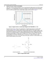
1 Supply Current vs. Control Input Voltage for the TS5A3159A (V
+
= 5 V) ............................................ 2
2 Simple CMOS Inverter ...................................................................................................... 2
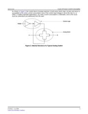
3 Internal Structure of a Typical Analog Switch ............................................................................ 3
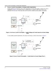
4 No Excess Current Consumption – Supply Voltage and Control Input Are at Same Voltage Level .............. 4
5 Excess Current Consumption – Control Input Is at Lower Voltage Than V
+
......................................... 4
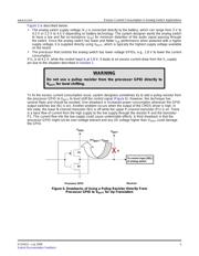
6 Drawbacks of Using a Pullup Resistor Directly From Processor GPIO to V
BATT
for Up-Translation .............. 5
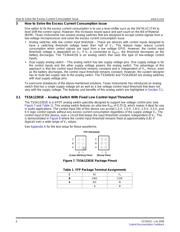
7 TS5A12301E Package Pinout ............................................................................................. 6
8 Control Input Threshold is Independent of V
+
............................................................................ 7
9 Input Threshold Variation on Competitor Device ........................................................................ 7
10 TS5A12301E Has a Constant Threshold Even as the Battery Discharges .......................................... 8
11 Comparison of Supply Current Between Competitor Solution and TS5A12301E ................................... 8
A-1 Test Setup for TS5A12301E (V
OUT
vs V
IN
) .............................................................................. 11
A-2 Test Setup for Competitor Device (V
OUT
vs V
IN
)........................................................................ 11
A-3 Test Setup for Supply Currrent vs Control Input Voltage ............................................................. 12
List of Tables
1 YFP Package Terminal Assignments ..................................................................................... 6
2 Summary of Power Consumption With Different Solutions ............................................................ 9
SCDA011 – July 2008 1
Submit Documentation Feedback
Verzeichnis