
herunterladen

Application Report
SLVA389–March 2010
TPS54620 Parallel Operation
John Tucker and Arvind Raj ...............................................................................................................
ABSTRACT
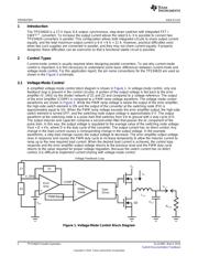
The TPS54620 is a synchronous, step-down, dc-dc converter with integrated high- and low-side FETs. It
is rated for a continuous output of 6 A. In order to increase the output current capability, it is possible to
operate two TPS54620 circuits in parallel. Certain techniques are required in the design to ensure that
each of the TPS54620 converters provides an equal share of the output current. This application report
details the design, operation, and performance of a parallel TPS54620 dc/dc converter.
Contents
1 Introduction .................................................................................................................. 2
2 Control Types ................................................................................................................ 2
3 Parallel Operation ........................................................................................................... 4
4 Design Procedure ........................................................................................................... 5
5 Performance ................................................................................................................. 8
6 Conclusion .................................................................................................................. 13
List of Figures
1 Voltage-Mode Control Block Diagram.................................................................................... 2
2 Voltage-Mode Control Waveforms........................................................................................ 3
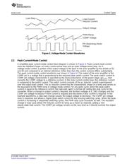
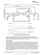
3 Peak Current-Mode Control Block Diagram............................................................................. 4
4 Peak Current-Mode Control Waveforms................................................................................. 4
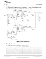
5 TPS54620 Example Design ............................................................................................... 5
6 TPS54620 Parallel Circuit Current Sharing.............................................................................. 9
7 TPS54620 Parallel Circuit Efficiency.................................................................................... 10
8 TPS54620 Parallel Circuit Output Voltage Ripple..................................................................... 10
9 TPS54620 Parallel Circuit Input Voltage Ripple....................................................................... 11
10 Switching Node and Inductor Current Waveforms.................................................................... 11
11 Closed-Loop Response................................................................................................... 12
12 Transient Response....................................................................................................... 13
List of Tables
1 Design Requirements ...................................................................................................... 5
1
SLVA389–March 2010 TPS54620 Parallel Operation
Submit Documentation Feedback
Copyright © 2010, Texas Instruments Incorporated
Verzeichnis
- ・ Blockdiagramm on Seite 2 Seite 4
- ・ Anwendungsbereich on Seite 14