
herunterladen

Application Report
SCAA052A – November 2001 – Revised April 2006
1
Using TI’s CDCV304 with Backplane Transceiver
(TLK1201, TLK1501, TLK2201, TLK2501, TLK2701,
TLK2711, and TLK3101)
Firoj Kabir HPA/CDC
ABSTRACT
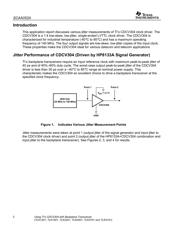
This application note discusses TI’s CDCV304 output jitter when driving serial backplane
transceivers, namely, TLK1201, TLK1501, TLK2201, TLK2501, TLK2701, TLK2711, and
TLK3101. Measurement shows that the CDCV304 clock driver generates 20-ps p-p jitter
on average; hence it is suitable to drive any serial backplane transceivers fulfilling all the
requirements.
Contents
Introduction .............................................................................................................................................2
Jitter Performance of CDCV304 (Driven by HP8133A Signal Generator) ..........................................2
Test Equipment Setup for Driving Backplane Transceiver.................................................................4
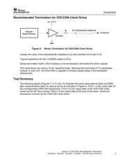
Recommended Termination for CDCV304 Clock Driver......................................................................5
Test Summary .........................................................................................................................................5
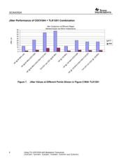
Jitter Performance of CDCV304 + TLK1201 Combination................................................................6
Jitter Performance of CDCV304 + TLK1501 Combination................................................................7
Jitter Performance of CDCV304 + TLK2501 Combination................................................................8
Jitter Performance of CDCV304 + TLK3101 Combination................................................................9
Conclusion ..............................................................................................................................................9
References.............................................................................................................................................10
Figures
Figure 1. Indicates Various Jitter Measurement Points ...................................................................2
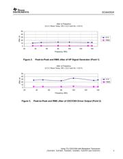
Figure 2. Peak-to-Peak and RMS Jitter of HP Signal Generator (Point 1) ......................................3
Figure 3. Peak-to-Peak and RMS Jitter of CDCV304 Driver Output (Point 2) .................................3
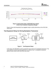
Figure 4. Peak-to-Peak Jitter of CDCV304 Driver Output (Point 2 Over Industrial
Temperature Range) ...........................................................................................................4
Figure 5. Test Equipment Setup .........................................................................................................4
Figure 6. Thevenin Termination for CDCV304 Clock Driver ............................................................5
Figure 7. Jitter Values at Different Points Shown in Figure 5 With TLK1201.................................6
Figure 8. Jitter Values at Different Points Shown in Figure 5 With TLK1501.................................7
Figure 9. Jitter Values at Different Points Shown in Figure 5 With TLK2501.................................8
Figure 10. Jitter Values at Different Points Shown in Figure 5 With TLK3101.................................9
Tables
Table 1. Recommended Clock Drivers for Serial / Gigabit Transceivers .........................................9