
Application Report
SLUA271A – June 2002 – Revised September 2007
QFN/SON PCB Attachment
Steve Kummerl, Bernhard Lange, Dominic Nguyen .................................................................................
ABSTRACT
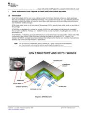
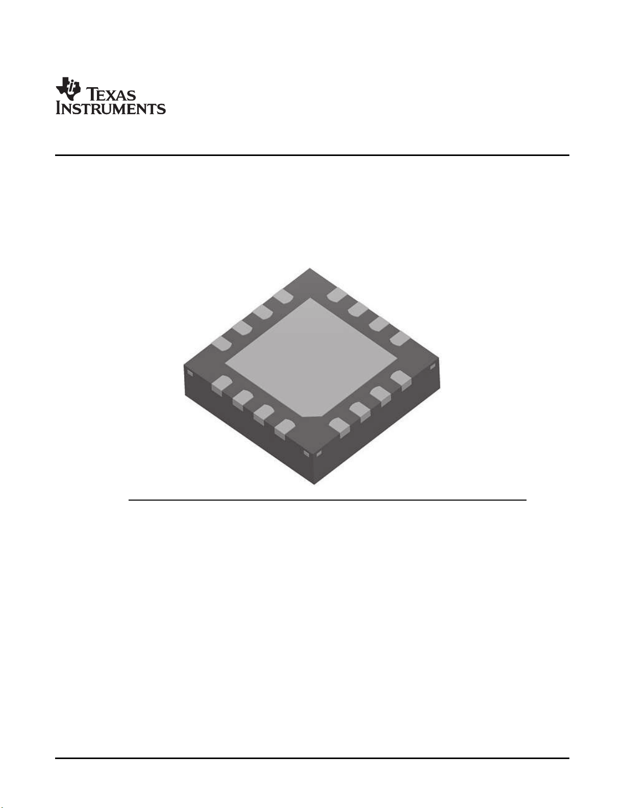
Quad flatpack no leads (QFNs) and small-outline no leads (SONs) are leadless
packages with electrical connections made via lands on the bottom side of the
component to the surface of the connecting substrate (PCB, ceramic). This application
report presents users with introductory information about attaching QFN/SON devices
to printed circuit boards (PCBs).
Contents
1 Texas Instruments Quad Flatpack No Leads and Small-Outline No Leads ................ 3
2 Manufacturing Considerations .................................................................... 4
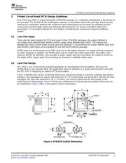
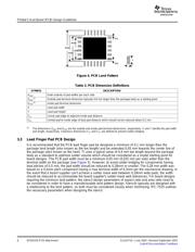
3 Printed Circuit Board (PCB) Design Guidelines ................................................ 5
4 Solder Paste Screen Printing Process ......................................................... 10
5 Package to Board Assembly Process .......................................................... 13
6 Rework Guidelines (Hot Gas Convection and Manual) ...................................... 16
List of Figures
1 QFN Structure ....................................................................................... 3
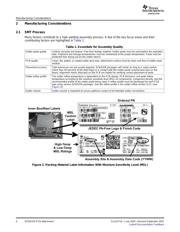
2 Packing Material Label Information With Moisture Sensitivity Level (MSL) ................. 4
3 QFN/SON Outline Dimensions .................................................................... 5
4 PCB Land Pattern .................................................................................. 6
5 Substrate/PCB Lead Finger Geometry .......................................................... 7
6 X-Ray Images for Reference ...................................................................... 8
7 Substrate/PCB Solder Mask and Keep-Out Area Example ................................... 8
8 Avoid Excessive Bending .......................................................................... 9
9 Solder Stencil Profile ............................................................................. 10
SLUA271A – June 2002 – Revised September 2007 QFN/SON PCB Attachment 1
Submit Documentation Feedback
Verzeichnis