
herunterladen
© Semiconductor Components Industries, LLC, 2013
September, 2013 − Rev. 10
1 Publication Order Number:
TIP41A/D
TIP41G, TIP41AG, TIP41BG,
TIP41CG (NPN),
TIP42G,TIP42AG, TIP42BG,
TIP42CG(PNP)
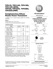
Complementary Silicon
Plastic Power Transistors
Designed for use in general purpose amplifier and switching
applications.
Features
• Epoxy Meets UL 94 V−0 @ 0.125 in
• These Devices are Pb−Free and are RoHS Compliant*
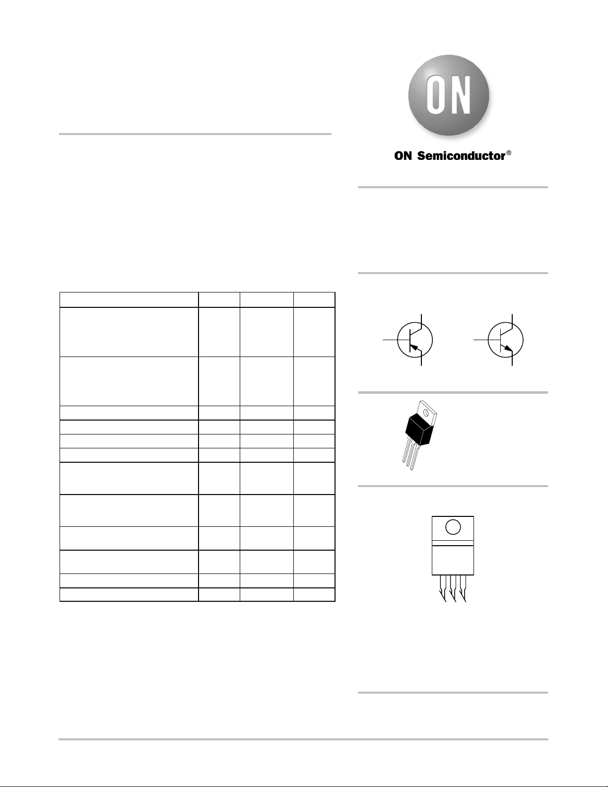
MAXIMUM RATINGS
Rating Symbol Value Unit
Collector−Emitter Voltage
TIP41G, TIP42G
TIP41AG, TIP42AG
TIP41BG, TIP42BG
TIP41CG, TIP42CG
V
CEO
40
60
80
100
Vdc
Collector−Base Voltage
TIP41G, TIP42G
TIP41AG, TIP42AG
TIP41BG, TIP42BG
TIP41CG, TIP42CG
V
CB
40
60
80
100
Vdc
Emitter−Base Voltage V
EB
5.0 Vdc
Collector Current − Continuous I
C
6.0 Adc
Collector Current − Peak I
CM
10 Adc
Base Current I
B
2.0 Adc
Total Power Dissipation
@ T
C
= 25°C
Derate above 25°C
P
D
65
0.52
W
W/°C
Total Power Dissipation
@ T
A
= 25°C
Derate above 25°C
P
D
2.0
0.016
W
W/°C
Unclamped Inductive Load Energy
(Note 1)
E 62.5 mJ
Operating and Storage Junction,
Temperature Range
T
J
, T
stg
–65 to +150 °C
ESD − Human Body Model HBM 3B V
ESD − Machine Model MM C V
Stresses exceeding Maximum Ratings may damage the device. Maximum
Ratings are stress ratings only. Functional operation above the Recommended
Operating Conditions is not implied. Extended exposure to stresses above the
Recommended Operating Conditions may affect device reliability.
1. I
C
= 2.5 A, L = 20 mH, P.R.F. = 10 Hz, V
CC
= 10 V, R
BE
= 100 W.
*For additional information on our Pb−Free strategy and soldering details, please
download the ON Semiconductor Soldering and Mounting Techniques
Reference Manual, SOLDERRM/D.
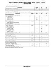
TO−220
CASE 221A
STYLE 1
MARKING DIAGRAM
6 AMPERE
COMPLEMENTARY SILICON
POWER TRANSISTORS
40−60−80−100 VOLTS,
65 WATTS
http://onsemi.com
1
2
3
4
TIP4xx = Device Code
xx = 1, 1A, 1B, 1C
2, 2A, 2B, 2C
A = Assembly Location
Y = Year
WW = Work Week
G = Pb−Free Package
TIP4xxG
AYWW
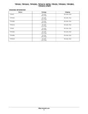
See detailed ordering and shipping information in the package
dimensions section on page 6 of this data sheet.
ORDERING INFORMATION
1
BASE
3
EMITTER
COLLECTOR
2,4
1
BASE
3
EMITTER
COLLECTOR
2,4
NPNPNP
Verzeichnis