
herunterladen
Semiconductor Components Industries, LLC, 2012
January, 2012 − Rev. 9
1 Publication Order Number:
MM3Z2V4T1/D
MM3ZxxxT1G Series,
SZMM3ZxxxT1G Series
Zener Voltage Regulators
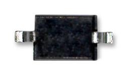
200 mW SOD−323 Surface Mount
This series of Zener diodes is packaged in a SOD−323 surface
mount package that has a power dissipation of 200 mW. They are
designed to provide voltage regulation protection and are especially
attractive in situations where space is at a premium. They are well
suited for applications such as cellular phones, hand held portables,
and high density PC boards.
Specification Features:
Standard Zener Breakdown Voltage Range − 2.4 V to 75 V
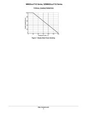
Steady State Power Rating of 200 mW
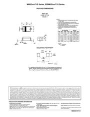
Small Body Outline Dimensions:
0.067” x 0.049” (1.7 mm x 1.25 mm)
Low Body Height: 0.035” (0.9 mm)
Package Weight: 4.507 mg/Unit
ESD Rating of Class 3 (> 16 kV) per Human Body Model
AEC−Q101 Qualified and PPAP Capable − SZMM3ZxxxT1G
SZ Prefix for Automotive and Other Applications Requiring Unique
Site and Control Change Requirements
These are Pb−Free Devices*
Mechanical Characteristics:
CASE: Void-free, Transfer-Molded Plastic
FINISH: All External Surfaces are Corrosion Resistant
MAXIMUM CASE TEMPERATURE FOR SOLDERING PURPOSES:
260C for 10 Seconds
LEADS: Plated with Pb−Sn or Sn Only (Pb−Free)
POLARITY: Cathode Indicated by Polarity Band
FLAMMABILITY RATING: UL 94 V−0
MOUNTING POSITION: Any
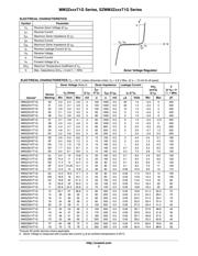
MAXIMUM RATINGS
Rating Symbol Max Unit
Total Device Dissipation FR−5 Board,
(Note 1) @ T
A
= 25C
Derate above 25C
P
D
200
1.5
mW
mW/C
Thermal Resistance, Junction−to−Ambient
R
q
JA
635 C/W
Junction and Storage Temperature Range T
J
, T
stg
−65 to +150 C
Stresses exceeding Maximum Ratings may damage the device. Maximum
Ratings are stress ratings only. Functional operation above the Recommended
Operating Conditions is not implied. Extended exposure to stresses above the
Recommended Operating Conditions may affect device reliability.
1. FR−4 Minimum Pad
*For additional information on our Pb−Free strategy and soldering details, please
download the ON Semiconductor Soldering and Mounting Techniques
Reference Manual, SOLDERRM/D.
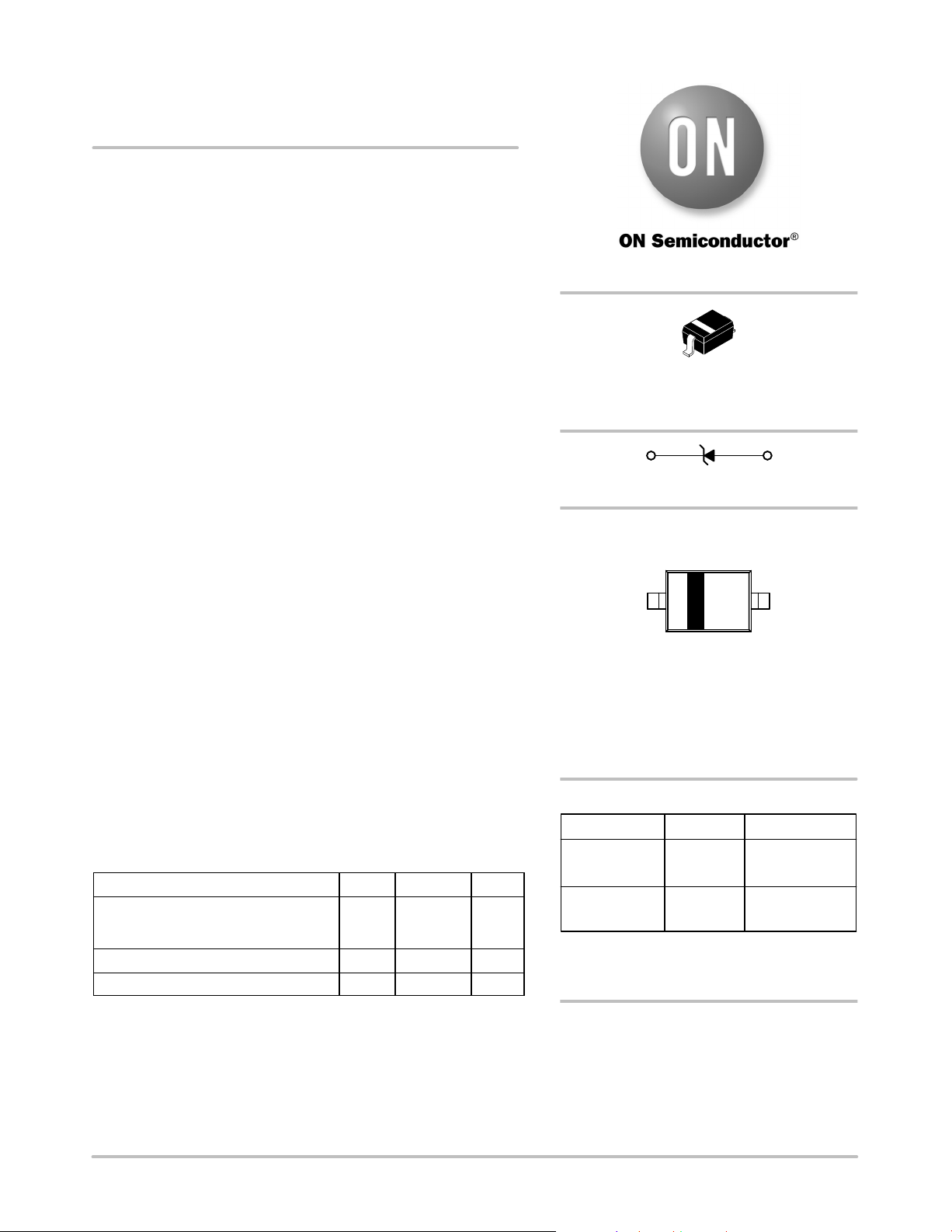
1
Cathode
2
Anode
See specific marking information in the device marking
column of the Electrical Characteristics table on page 2 of
this data sheet.
DEVICE MARKING INFORMATION
Device Package Shipping†
ORDERING INFORMATION
MARKING DIAGRAM
†For information on tape and reel specifications,
including part orientation and tape sizes, please
refer to our Tape and Reel Packaging Specifications
Brochure, BRD8011/D.
MM3ZxxxT1G SOD−323
(Pb−Free)
3,000 /
Tape & Reel
http://onsemi.com
SOD−323
CASE 477
STYLE 1
(Note: Microdot may be in either location)
xx G
G
M
*Date Code orientation may vary depending
upon manufacturing location.
xx = Specific Device Code
M = Date Code*
G = Pb−Free Package
SZMM3ZxxxT1G SOD−323
(Pb−Free)
3,000 /
Tape & Reel
Verzeichnis