
herunterladen
1/9
AN1453
APPLICATION NOTE
®
NEW FAMILY OF 150V POWER SCHOTTKY
July 2001
By F. GAUTIER
Nowadays, the Switch Mode Power Supply
(SMPS) is becoming more widespread as a result
of computer, telecom and consumer applications.
The constant increase in services (more
peripherals) and performance, which offers us
these applications, tends to move conversion
systems towards higher output power.
In addition to these developments dictated by the
market, SMPS manufacturers are in competition,
their battlefield being the criteria of power density,
efficiency, reliability and cost, this last being factor
very critical.
Today, SMPS designers of 12V-24V output have
practically the choice between a 100V Schottky or
a 200V bipolar diode.
The availability of an intermediate voltage has
become necessary to gain in design optimization.
This is why STMicroelectronics is introducing a
new family of 150V POWER SCHOTTKY diodes,
intendedfor 12Vandmore secondaryrectification,
in applications such as desktops, file servers or
adaptors for notebook.
Consequently, this application note will underline
the advantages of a 150V Schottky technology
compared to a 200V ultra fast diode.
In order to do this, the example of a Flyback
converter will be used, and the static and dynamic
parameters of the 150V Schottky will be detailed,
as well as their influence in this converter.
1.CONDUCTIONLOSSES&EFFICIENCYGAIN
Schottky diodes are mainly used for output
rectification. In a typical SMPS working with a
switching frequency lower than 100kHz,
conduction losses are generally themain losses in
the diode. They are directly linked to the curve of
forward voltage (V
F
) versus forward current (I
F
),
and obviously the best gain in efficiency will be
obtained with the lowest V
F
.
In the following examples, the conduction losses
between a 150V Schottky and a 200V bipolar
diode in a Flyback and a Forward converter will be
compared.
The conduction losses in the diode are calculated
from the classical formula:
P=VI+RI
cond T0 F(AV) d IF(RMS)
2
⋅⋅
V :threshold voltage with V = V +R .I
t0 F(@IF) T0 d F
R : dynamic resistance with R = V / I
ddFF
∆∆
where V
T0
and R
d
are calculated from the current
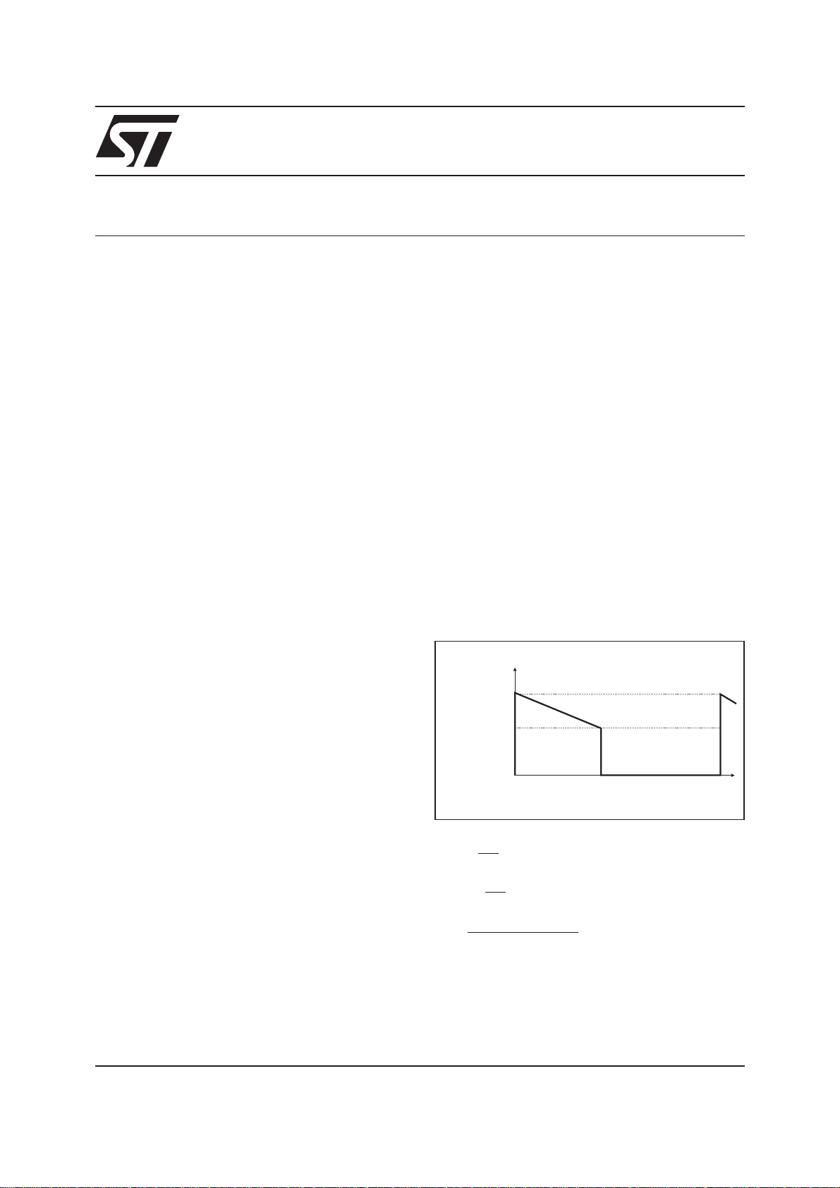
range of current view by the diode (Fig. 1), for
better accuracy.
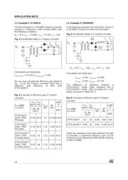
Figure 1 shows also, the typical current through
the rectification diode and the corresponding I
F(AV)
and
I
IF(RMS)
2
:
I=(I I)
I(III
F(AV)
ID
max min
F(RMS)
2
ID
max min
2
m
α
α
2
3
2
+
=++
ax min
d
F(@Imax) F(@Imin)
max min
T0 F
I
R=
VV
II
VV
⋅
−
−
=
)
(@imax) d max
RI−⋅
NB:
-In the datasheet, the V
T0
and R
d
are maximum
values given for I
F
and2I
F
at 125°C.
-In discontinuous mode I
min
=0.
I
D
0
αI.T
D
I
min
T
t
I
ma x
Fig. 1: Typical current through a rectification diode
INTRODUCTION