
herunterladen
DC Electrical
Characteristics of MM74HC
High-Speed CMOS Logic
The input and output characteristics of the MM74HC
high-speed CMOS logic family were conceived to meet sev-
eral basic goals. These goals are to provide input current
and voltage requirements, noise immunity and quiescent
power dissipation similar to CD4000 and MM74C metal-gate
CMOS logic and output current drives similar to low power
Schottky TTL. In addition, to enable merging of TTL and
HC-CMOS designs, the MM74HCT sub family differs only in
their input voltage requirements, which are the same asTTL,
to ease interfacing between logic families.
In order to familiarize the user with the MM74HC logic family,
its input and output characteristics are discussed in this ap-
plication note, as well as how these characteristics are af-
fected by various parameters such as power supply voltage
and temperature. Also, for those users who have been de-
signing with metal-gate CMOS and TTL logic, notable differ-
ences and features of high-speed CMOS are compared to
those logic families.
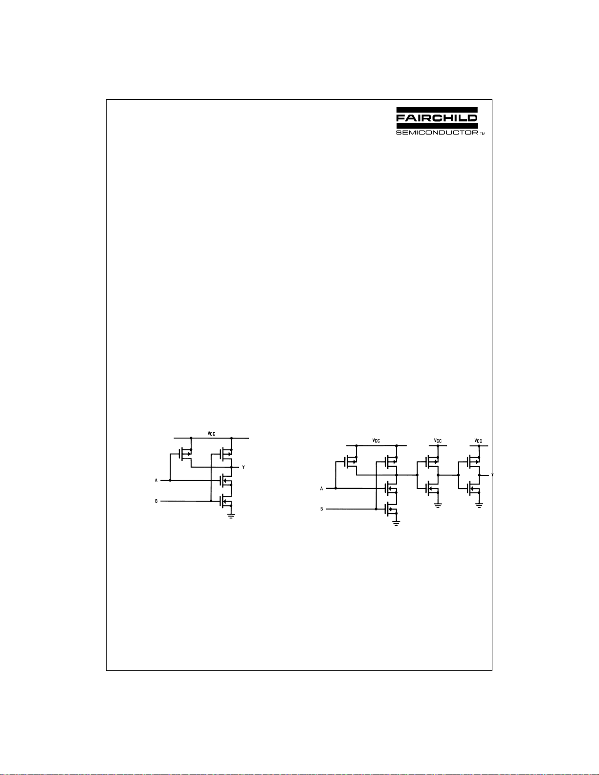
A Buffered CMOS Logic Family
The MM74HC is a “buffered” logic family like the CD4000B
series CMOS. Buffering CMOS logic merely denotes design-
ing the IC so that the output is taken from an inverting buffer
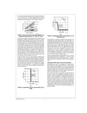
stage. For example, the internal circuit implementation of a
NAND gate would be a simple NAND followed by two invert-
ing stages. An unbuffered gate would be implemented as a
single stage. Both are shown in
Figure 1
. Most MSI logic de-
vices are inherently buffered because they are inherently
multi-stage circuits. Gates and similar small circuits yield the
greatest improvement in performance by buffering.
There are several advantages to buffering this high-speed
CMOS family. By using a standardized buffer, the output
characteristics for all devices are more easily made identical.
Multi-stage gates will have better noise immunity due to the
higher gain caused by having several stages from input to
output. Also, the output impedance of an unbuffered gate
may change with input logic level voltage and input logic
combination, whereas buffered outputs are unaffected by in-
put conditions.
Finally, single stage gates implemented in MM74HC CMOS
would require large transistors due to the large output drive
requirements. These large devices would have a large input
capacitance associated with them. This would affect the
speed of circuits driving into an unbuffered gate, especially
when driving large fanouts. Buffered gates have small input
transistors and correspondingly small input capacitance.
One may think that a major disadvantage of buffered circuits
would be speed loss. It would seem that a two or three stage
gate would be two to three times slower than a buffered one.
However, internal stages are much faster than the output
stage and the speed lost by buffering is relatively small.
The one exception to buffering is the MM74HCU04 hex in-
verter which is unbuffered to enable its use in various linear
and crystal oscillator applications.
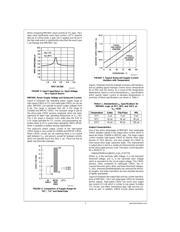
CMOS Input Voltage Characteristics
As mentioned before, MM74HC standard input levels are
similar to metal-gate CMOS. This enables the high-speed
logic family to enjoy the same wide noise margin of CD4000
and MM74C logic. With V
CC
=
5V these input levels are 3.5V
for minimum logic “1” (V
IH
) and 1.0V for a logic “0” (V
IL
). The
output levels when operated at V
CC
=
5V
±
10
%
and worst
case input levels, are specified to be V
CC
−0.1 or 0.1V. The
output levels will actually be within a few millivolts of either
V
CC
or ground.
When operated over the entire supply voltage range, the in-
put logic levels are: V
IH
=
0.7V
CC
and V
IL
=
0.2V
CC
.
Figure 2
il-
lustrates the input voltage levels and the noise margin of
these circuits over the power supply range. The shaded area
indicates the noise margin which is the difference between
the input and output logic levels. The logic “1” noise margin
is 29
%
of V
CC
and the logic “0” noise margin is 19
%
of V
CC
.
Also shown for comparison are the 74LS input levels and
noise margins over their supply range.
AN005052-1
(a)
AN005052-2
(b)
FIGURE 1. Schematic Diagrams of (a) Unbuffered and (b) Buffered NAND Gate
Fairchild Semiconductor
Application Note 313
Larry Wakeman
April 1998
DC Electrical Characteristics of MM74HC High-Speed CMOS Logic AN-313
© 1998 Fairchild Semiconductor Corporation AN005052 www.fairchildsemi.com
Verzeichnis