
herunterladen
© Semiconductor Components Industries, LLC, 2011
November, 2017 − Rev. 8
1 Publication Order Number:
SMS05C/D
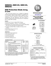
SMS05C, SMS12C, SMS15C,
SMS24C
ESD Protection Diode Array,
5-Line
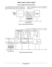
This 5−line surge protection array is designed for application
requiring transient voltage protection capability. It is intended for use
in over−transient voltage and ESD sensitive equipment such as
computers, printers, automotive electronics, networking
communication and other applications. This device features a
monolithic common anode design which protects five independent
lines in a single TSOP−6 package.
Features
• Protects up to 5 Lines in a Single TSOP−6 Package
• Peak Power Dissipation − 350 W (8 20 ms Waveform)
• ESD Rating of Class 3B (Exceeding 8.0 kV) per Human Body Model
and Class C (Exceeding 400 V) per Machine Model
• Compliance with IEC 61000−4−2 (ESD) 15 kV (Air), 8.0 kV
(Contact)
• Flammability Rating of UL 94 V−0
• These are Pb−Free Devices
Applications
• Hand−Held Portable Applications
• Networking and Telecom
• Automotive Electronics
• Serial and Parallel Ports
• Notebooks, Desktops, Servers
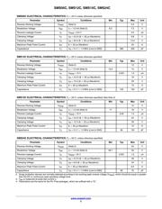
MAXIMUM RATINGS (T
J
= 25°C unless otherwise specified)
Symbol
Rating Value Unit
P
PK
1 Peak Power Dissipation
8 20 ms Double Exponential Waveform
(Note 1)
350 W
T
J
Operating Junction Temperature Range −40 to 150 °C
T
STG
Storage Temperature Range −55 to 150 °C
T
L
Lead Solder Temperature (10 s) 260 °C
ESD Human Body Model ( HBM)
Machine Model (MM)
IEC 61000−4−2 Air (ESD)
IEC 61000−4−2 Contact (ESD)
>8000
>400
>15000
>8000
V
Stresses exceeding those listed in the Maximum Ratings table may damage the
device. If any of these limits are exceeded, device functionality should not be
assumed, damage may occur and reliability may be affected.
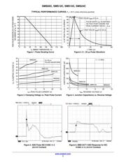
1. Non−repetitive current pulse per Figure 3.
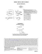
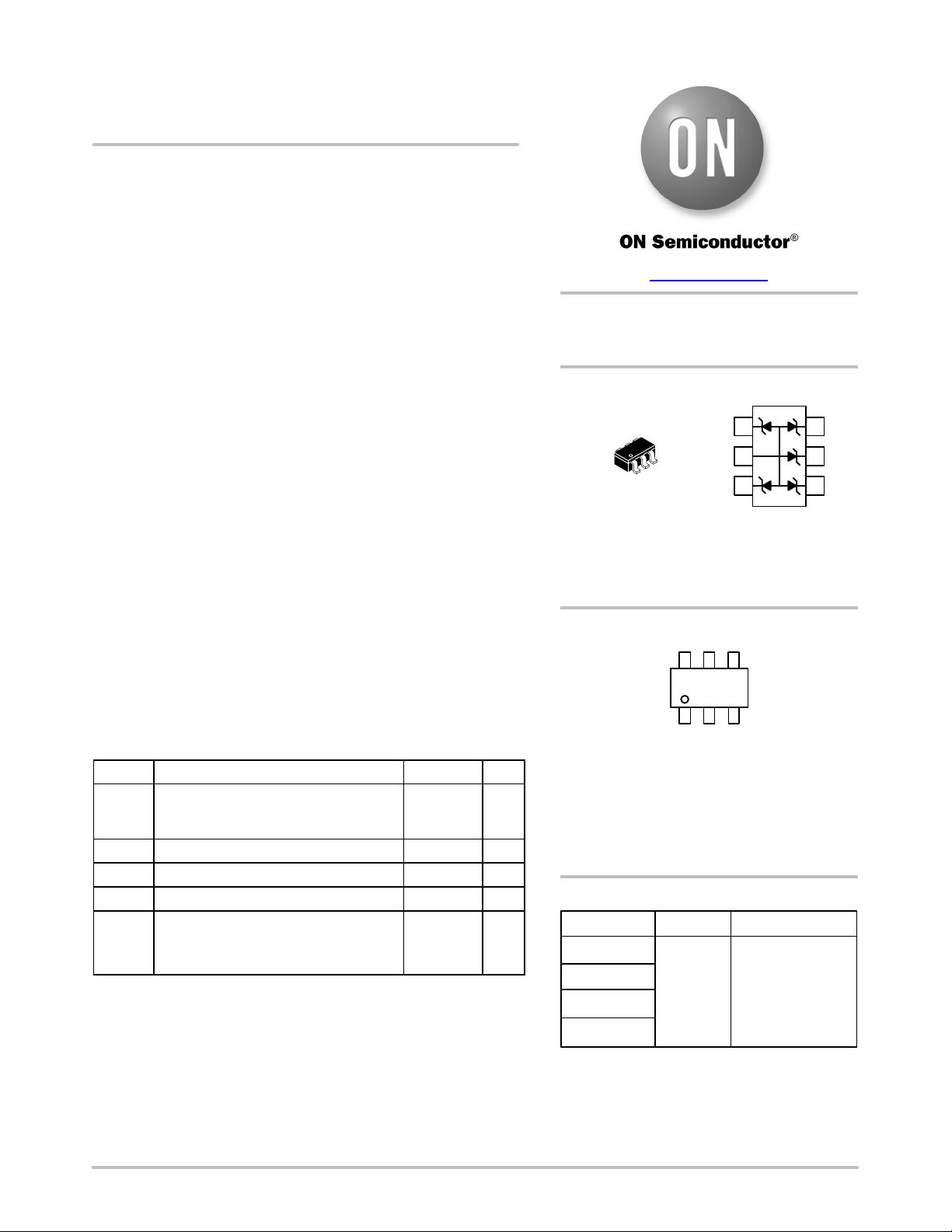
TSOP−6 FIVE SURGE
PROTECTION
350 W PEAK POWER
TSOP−6
CASE 318G
1
2
3
6
5
4
MARKING DIAGRAM
PIN ASSIGNMENT
Device Package Shipping
†
ORDERING INFORMATION
SMS05CT1G
PIN 1. CATHODE
2. ANODE
3. CATHODE
4. CATHODE
5. CATHODE
6. CATHODE
www.onsemi.com
1
6
6x MG
G
x = SMS05C:J
= SMS12C:K
= SMS15C:L
= SMS24C:M
M
= Date Code
G = Pb−Free Package
SMS12CT1G
SMS15CT1G
TSOP−6
(Pb−Free)
3000/Tape & Reel
†For information on tape and reel specifications,
including part orientation and tape sizes, please
refer to our Tape and Reel Packaging Specification
Brochure, BRD8011/D.
SMS24CT1G
www.onsemi.com
(Note: Microdot may be in either location)
SCALE 2:1
Verzeichnis
- ・ Konfiguration des Pinbelegungsdiagramms on Seite 1
- ・ Abmessungen des Paketumrisses on Seite 5
- ・ Paket-Footprint-Pad-Layout on Seite 5
- ・ Teilenummerierungssystem on Seite 1 Seite 5
- ・ Markierungsinformationen on Seite 1 Seite 5
- ・ Anwendungsbereich on Seite 1 Seite 4
- ・ Elektrische Spezifikation on Seite 2
- ・ Teilenummernliste on Seite 1