
herunterladen
Semiconductor Components Industries, LLC, 2012
February, 2012 − Rev. 4
1 Publication Order Number:
SMF05C/D
SMF05CT1G, SMF12CT1G,
SMF15CT1G, SMF24CT1G,
SZSMF12CT1G
5-Line Transient Voltage
Suppressor Array
This 5−line voltage transient suppressor array is designed for
application requiring transient voltage protection capability. It is
intended for use in over−transient voltage and ESD sensitive
equipment such as computers, printers, automotive electronics,
networking communication and other applications. This device
features a monolithic common anode design which protects five
independent lines in a single SC−88 package.
Features
Protects up to 5−Line in a Single SC−88 Package
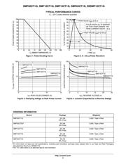
Peak Power Dissipation − 100 W (8 x 20 ms Waveform)
ESD Rating of Class 3B (Exceeding 8 kV) per Human Body Model
and Class C (Exceeding 400 V) per Machine Model.
Compliance with IEC 61000−4−2 (ESD) 15 kV (Air), 8 kV (Contact)
Flammability Rating of UL 94 V−0
SZ Prefix for Automotive and Other Applications Requiring Unique
Site and Control Change Requirements; AEC−Q101 Qualified and
PPAP Capable
Pb−Free Packages are Available*
Applications
Hand−Held Portable Applications
Networking and Telecom
Automotive Electronics
Serial and Parallel Ports
Notebooks, Desktops, Servers
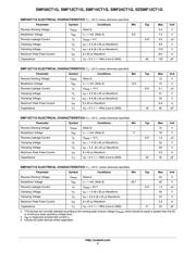
MAXIMUM RATINGS (T
J
= 25C unless otherwise specified)
Symbol Rating Value Unit
P
PK
1 Peak Power Dissipation
8 x 20 ms Double Exponential Waveform
(Note 1)
100
W
T
J
Operating Junction Temperature Range −40 to 125 C
T
STG
Storage Temperature Range −55 to 150 C
T
L
Lead Solder Temperature (10 s) 260 C
ESD Human Body Model (HBM)
Machine Model (MM)
IEC 61000−4−2 Air (ESD)
IEC 61000−4−2 Contact (ESD)
16000
400
15000
15000
V
Stresses exceeding Maximum Ratings may damage the device. Maximum
Ratings are stress ratings only. Functional operation above the Recommended
Operating Conditions is not implied. Extended exposure to stresses above the
Recommended Operating Conditions may affect device reliability.
1. Nonrepetitive current pulse per Figure 3.
*For additional information on our Pb−Free strategy and soldering details, please
download the ON Semiconductor Soldering and Mounting Techniques
Reference Manual, SOLDERRM/D.
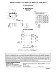
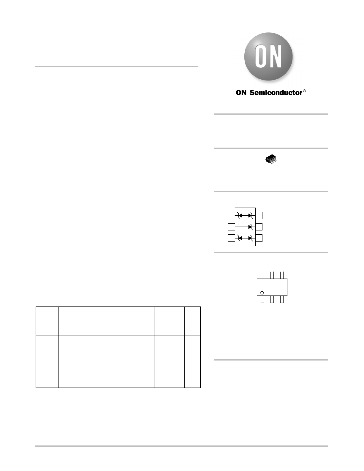
SC−88 FIVE TRANSIENT
VOLTAGE SUPPRESSOR
100 W PEAK POWER
SC−88
CASE 419B
STYLE 24
1
2
3
6
5
4
MARKING DIAGRAM
PIN ASSIGNMENT
PIN 1. CATHODE
2. ANODE
3. CATHODE
4. CATHODE
5. CATHODE
6. CATHODE
http://onsemi.com
XX = Specific Device Code
6J = SMF05C
6K = SZSMF12C/SMF12C
6L = SMF15C
6M= SMF24C
M = Date Code
G =Pb−Free Package
XX
M
G
G
1
6
See detailed ordering and shipping information in the package
dimensions section on page 3 of this data sheet.
ORDERING INFORMATION
Verzeichnis
- ・ Konfiguration des Pinbelegungsdiagramms on Seite 1
- ・ Abmessungen des Paketumrisses on Seite 4
- ・ Paket-Footprint-Pad-Layout on Seite 4
- ・ Teilenummerierungssystem on Seite 1 Seite 3 Seite 4
- ・ Markierungsinformationen on Seite 1
- ・ Technische Daten on Seite 3
- ・ Anwendungsbereich on Seite 1
- ・ Elektrische Spezifikation on Seite 2