

herunterladen
Copyright © 2000, Texas Instruments Incorporated SBOA081 Printed in U.S.A. November, 2000
CURRENT FEEDBACK AMPLIFIERS:
REVIEW, STABILITY ANALYSIS, AND APPLICATIONS
By John Austin
INTRODUCTION
Many Engineers still refuse to design with Current FeedBack
(CFB) amplifiers. This is due to a few misunderstandings,
which can be easily clarified.
The majority of op amp circuits are closed-loop feedback
systems that implement classical control theory analysis.
Analog designers are comfortable with Voltage FeedBack
(VFB) op amps in a closed-loop system and are familiar with
the ideal op amp approximations feedback permit. This
application bulletin will demonstrate how CFB op amps can
be analyzed in a similar fashion. Once the closed-loop
similarities are understood, it is easy to see that most circuits
commonly built with VFB amplifiers can utilize CFB ampli-
fiers, yielding better results at high frequencies.
REVIEW
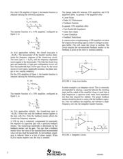
Figure 1 illustrates the open-loop terminal characteristics of
a VFB amplifier. Ideally both the inverting and non-invert-
ing inputs have infinite impedance. The output is a voltage
source with zero impedance. The potential difference be-
tween the inverting and non-inverting inputs controls the
voltage source (A(s)). Feedback drives this potential differ-
ence to zero.
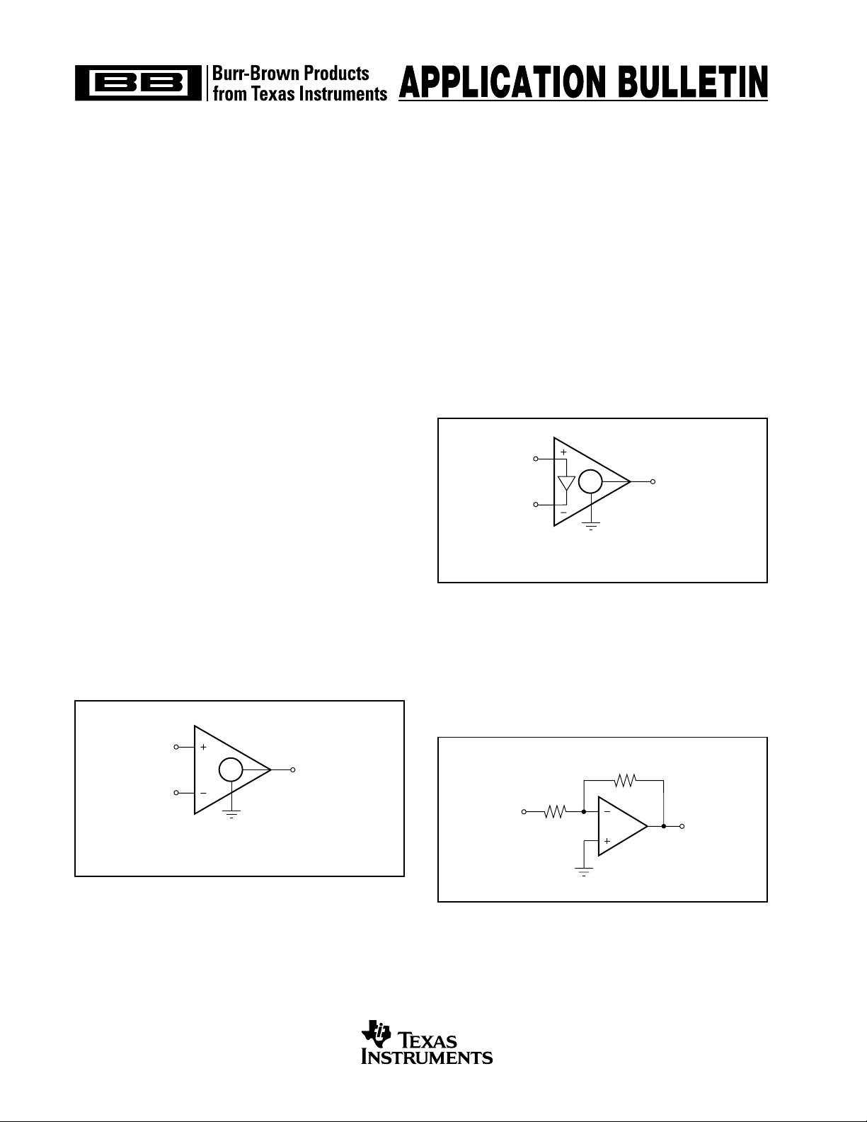
Figure 2 displays the terminal characteristics of a CFB
amplifier. Ideally the unity gain buffer, between the inputs
of the amplifier, cause the non-inverting input impedance
too be infinite while the inverting input impedance is zero.
The output impedance is zero, due to the voltage source. The
current out of the inverting input controls the voltage source
(Z(s)). Feedback forces this current to zero.
FIGURE 1. VFB Op Amp Model.
FIGURE 2. CFB Op Amp Model.
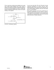
Figure 3 shows the basic configuration for inverting gain.
This circuit holds true for both CFB and VFB amplifiers. A
point to remember is that the value of the feedback resistor
is limited for CFB amplifiers. A recommended value will be
provided in the data sheet.
FIGURE 3. Inverting Gain Circuit.
V
1
V
O
V
2
A
(s)
Assumptions:
Z+ = ∞
Z– = ∞
Z
O
= 0
V
O
= A(s)[V
1
-V
2
]
V
1
V
O
V
2
Z (s)
Assumptions:
Z+ = ∞
Z– = 0
Z
O
= 0
V
O
= Z(s)I
INV
V
O
R
i
R
2
V
IN