
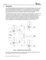
herunterladen

Application Report
SLOA100 - November 2002
1
Active Output Impedance for ADSL Line Drivers
Randy Stephens
Member Group Technical Staff
Broadband Amplifiers Systems Specialist
High Performance Linear Products
ABSTRACT
Signal termination is very common in bidirectional communication systems. Termination
allows for receiving signals while transmitting different signals at the same time. With the
increasing popularity of asymmetrical digital subscriber lines (ADSL), the requirement for a
low power line driver amplifier combined with line termination becomes a very difficult goal.
This application note examines the line driver amplifier requirements of an ADSL system and
how to utilize active impedance to obtain low power dissipation. Actual lab measurements
with a THS6032 line driver are discussed. Additionally, the receiver amplifier circuit
requirements and the system’s noise requirements are discussed with a THS6062 low-noise
amplifier used as an example.
Contents
1 Introduction 4. . . . . . . . . . . . . . . . . . . . . . . . . . . . . . . . . . . . . . . . . . . . . . . . . . . . . . . . . . . . . . . . . . . . . . . . .
2 Traditional Line Driver Requirements 5. . . . . . . . . . . . . . . . . . . . . . . . . . . . . . . . . . . . . . . . . . . . . . . . . .
2.1 Amplifier Output Voltages 5. . . . . . . . . . . . . . . . . . . . . . . . . . . . . . . . . . . . . . . . . . . . . . . . . . . . . . . . . .
2.2 Line Driver Power Dissipation 6. . . . . . . . . . . . . . . . . . . . . . . . . . . . . . . . . . . . . . . . . . . . . . . . . . . . . .
2.3 Minimizing Power Dissipation 7. . . . . . . . . . . . . . . . . . . . . . . . . . . . . . . . . . . . . . . . . . . . . . . . . . . . . .
2.4 Active Termination 8. . . . . . . . . . . . . . . . . . . . . . . . . . . . . . . . . . . . . . . . . . . . . . . . . . . . . . . . . . . . . . . .
2.5 Active Impedance Forward Gain 10. . . . . . . . . . . . . . . . . . . . . . . . . . . . . . . . . . . . . . . . . . . . . . . . . . .
2.6 Minimum Active Impedance Forward Gain Design Constraint 11. . . . . . . . . . . . . . . . . . . . . . . . . .
2.7 Line Impedance Changes 12. . . . . . . . . . . . . . . . . . . . . . . . . . . . . . . . . . . . . . . . . . . . . . . . . . . . . . . .
2.8 Line Impedance Changes and the Amplifier Output Voltage 14. . . . . . . . . . . . . . . . . . . . . . . . . . .
2.9 Line Impedance Changes and the Power on the Line 15. . . . . . . . . . . . . . . . . . . . . . . . . . . . . . . . .
2.10 General Conclusions—Introduction and System Requirements 16. . . . . . . . . . . . . . . . . . . . . . . .
3 Lab Tests 16. . . . . . . . . . . . . . . . . . . . . . . . . . . . . . . . . . . . . . . . . . . . . . . . . . . . . . . . . . . . . . . . . . . . . . . . . .
3.1 Lab Test Setup and the Transformers 17. . . . . . . . . . . . . . . . . . . . . . . . . . . . . . . . . . . . . . . . . . . . . .
3.2 Lab Tests—The Active Impedance Test 19. . . . . . . . . . . . . . . . . . . . . . . . . . . . . . . . . . . . . . . . . . . . .
3.3 Lab Tests—Power Dissipation and Power Supply Voltage 21. . . . . . . . . . . . . . . . . . . . . . . . . . . . .
3.4 Lab Tests—Power Dissipation and Distortion With a 1:1.2 Transformer 22. . . . . . . . . . . . . . . . .
3.5 Lab Tests—Power Dissipation and Distortion With a 1:1.42 Transformer 25. . . . . . . . . . . . . . . .
3.6 Lab Tests—Power Dissipation With Multiple Transformer Ratios 26. . . . . . . . . . . . . . . . . . . . . . .
3.7 Lab Tests—MTPR Distortion With Multiple Transformer Ratios 29. . . . . . . . . . . . . . . . . . . . . . . .
3.8 General Conclusions—Section 3—Lab Tests 31. . . . . . . . . . . . . . . . . . . . . . . . . . . . . . . . . . . . . . . .
4 The Receiver and Noise 31. . . . . . . . . . . . . . . . . . . . . . . . . . . . . . . . . . . . . . . . . . . . . . . . . . . . . . . . . . . . .
4.1 The Receive Signal Path—Summing Node Configuration 32. . . . . . . . . . . . . . . . . . . . . . . . . . . . .
Trademarks are the property of their respective owners.