

herunterladen
Publication Order Number:
NTF3055–100/D
Semiconductor Components Industries, LLC, 2001
July, 2001 – Rev. 0
1
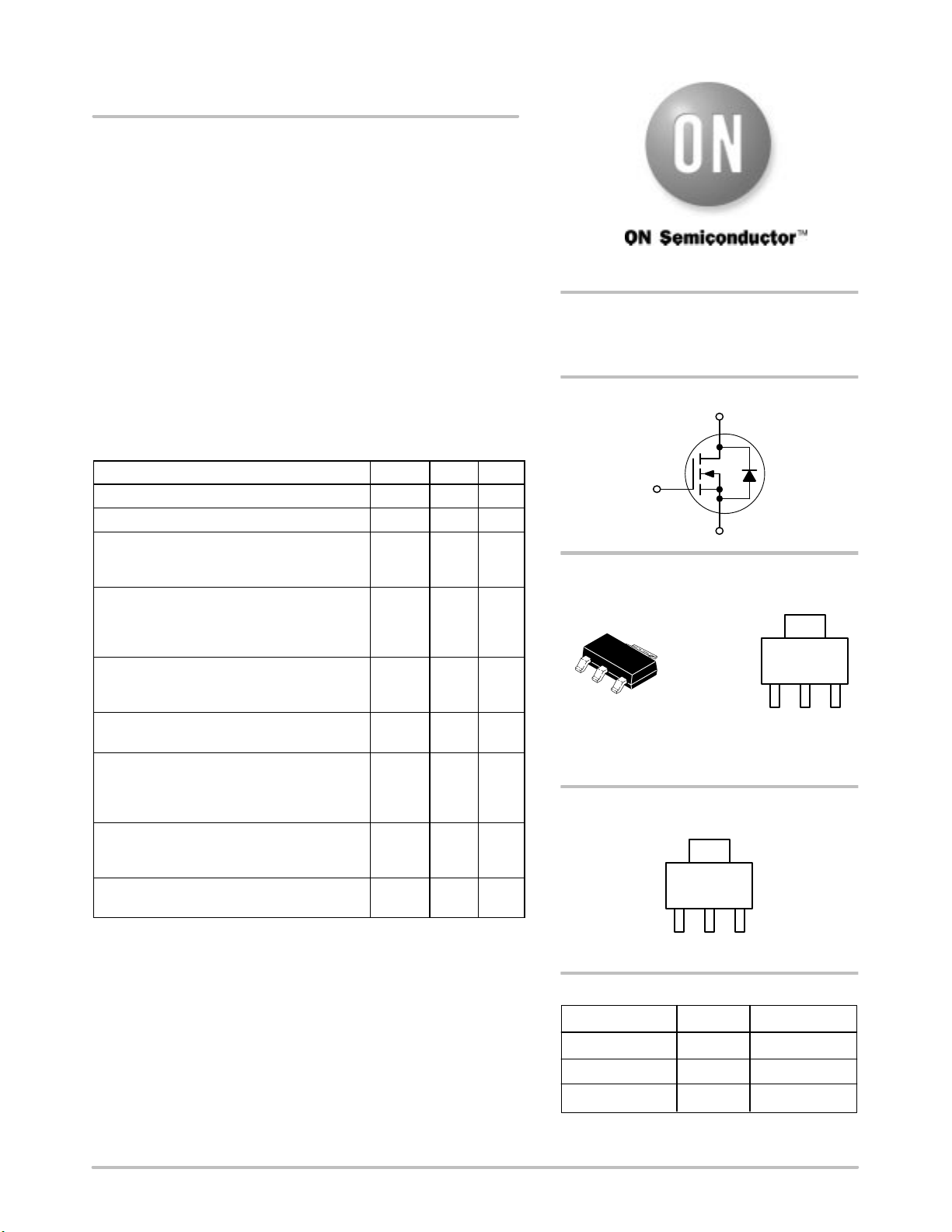
NTF3055-100
Preferred Device
Power MOSFET
3.0 Amps, 60 Volts
N–Channel SOT–223
Designed for low voltage, high speed switching applications in
power supplies, converters and power motor controls and bridge
circuits.
Applications
• Power Supplies
• Converters
• Power Motor Controls
• Bridge Circuits
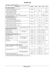
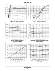
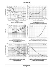
MAXIMUM RATINGS (T
C
= 25°C unless otherwise noted)
Rating
Symbol Value Unit
Drain–to–Source Voltage V
DSS
60 Vdc
Drain–to–Gate Voltage (R
GS
= 10 MΩ) V
DGR
60 Vdc
Gate–to–Source Voltage
– Continuous
– Non–repetitive (t
p
≤ 10 ms)
V
GS
± 20
± 30
Vdc
Vpk
Drain Current
– Continuous @ T
A
= 25°C
– Continuous @ T
A
= 100°C
– Single Pulse (t
p
≤ 10 µs)
I
D
I
D
I
DM
3.0
1.4
9.0
Adc
Apk
Total Power Dissipation @ T
A
= 25°C (Note 1.)
Total Power Dissipation @ T
A
= 25°C (Note 2.)
Derate above 25°C
P
D
2.1
1.3
0.014
W
W
W/°C
Operating and Storage Temperature Range T
J
, T
stg
–55 to
175
°C
Single Pulse Drain–to–Source Avalanche
Energy – Starting T
J
= 25°C
(V
DD
= 25 Vdc, V
GS
= 10 Vdc,
I
L
(pk) = 7.0 Apk, L = 3.0 mH, V
DS
= 60 Vdc)
E
AS
74 mJ
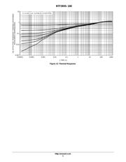
Thermal Resistance
– Junction to Ambient (Note 1.)
– Junction to Ambient (Note 2.)
R
θJA
R
θJA
72.3
114
°C/W
Maximum Lead Temperature for Soldering
Purposes, 1/8″ from case for 10 seconds
T
L
260 °C
1. When surface mounted to an FR4 board using 1″ pad size, 1 oz. (Cu. Area
1.127 in
2
).
2. When surface mounted to an FR4 board using minimum recommended pad
size, 2–2.4 oz. (Cu. Area 0.272 in
2
).
D
G
S
1
2
3
4
3.0 AMPERES
60 VOLTS
R
DS(on)
= 100 m
N–Channel
Device Package Shipping
ORDERING INFORMATION
NTF3055–100T1 SOT–223 1000 Tape & Reel
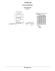
SOT–223
CASE 318E
STYLE 3
http://onsemi.com
LWW
MARKING
DIAGRAM
3055
3055 = Device Code
L = Location Code
WW = Work Week
PIN ASSIGNMENT
321
4
Gate Drain Source
Drain
NTF3055–100T3 SOT–223 4000 Tape & Reel
NTF3055–100T3LF SOT–223 4000 Tape & Reel
Verzeichnis