


herunterladen
MRFE6VP6600N MRFE6VP6600GN
1
RF Device Data
Freescale Semiconductor, Inc.
RF Power LDMOS Transistors
High Ruggedness N--Channel
Enhancement--Mode Lateral MOSFETs
These high ruggedness devices are designed for use in high VSWR
industrial, medical, broadcast, aerospace, and mobile radio applications. Their
unmatched input and output design allows for wide f requenc y r ange use from
1.8 to 600 MHz.
Typical Performance:
V
DD
=50Vdc
Frequency
(MHz)
Signal Type
P
out
(W)
G
ps
(dB)
D
(%)
87.5–108
(1,3)
CW 600 CW 24.0 81.8
230
(2)
Pulse
(100 sec, 20% Duty Cycle)
600 Peak 24.7 73.5
Load Mismatch/Ruggedness
Frequency
(MHz)
Signal Type VSWR
P
in
(W)
Test
Voltage
Result
230
(2)
Pulse
(100 sec, 20%
Duty Cycle)
> 65:1 at all
Phase Angles
4.0 Peak
(3 dB
Overdrive)
50 No Device
Degradation
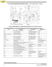
1. Measured in 87.5–108 MHz broadband reference circuit.
2. Measured in 230 MHz narrowband production test circuit.
3. The values shown are the center band performance numbers across the indicated
frequency range.
Features
Unmatched Input and Output Allowing Wide Frequency Range Utilization
Device can be used Single--Ended or in a Push--Pull Configuration
Qualified up to a Maximum of 50 V
DD
Operation
Characterized from 30 to 50 V for Extended Power Range
Suitable for Linear Application with Appropriate Biasing
Integrated ESD Protection with Greater Negative Gate--Source Voltage Range
for Improved Class C Operation
Characterized with Series Equivalent Large--Signal Impedance Parameters
Recommended drivers: AFT05MS004N (4 W) or MRFE6VS25N (25 W)
Typical Applications
Broadcast
– FM broadcast
– HF and VHF broadcast
Industrial, Scientific, Medical (ISM)
–CO
2
laser generation
– Plasma etching
– Particle accelerators (synchrotrons)
–MRI
– Industrial heating/welding
Aerospace
– VHF omnidirectional range (VOR)
– Weather radar
Mobile Radio
– HF and VHF communications
– PMR base stations
Document Number: MRFE6VP6600N
Rev. 0, 5/2015
Freescale Semiconductor
Technical Data
1.8–600 MHz, 600 W CW, 50 V
WIDEBAND
RF POWER LDMOS TRANSISTORS
MRFE6VP6600N
MRFE6VP6600GN
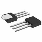
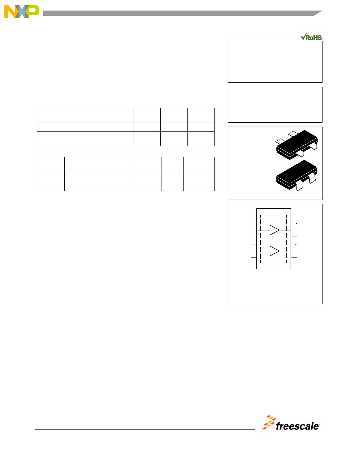
(Top View)
Figure 1. Pin Connections
Note: Exposed backside of the package is
the source terminal for the transistors.
OM--780G--4L
PLASTIC
MRFE6VP6600GN
Drain A
31
42
Drain B
Gate A
Gate B
OM--780--4L
PLASTIC
MRFE6VP6600N
Freescale Semiconductor, Inc., 2015. All rights reserved.
Verzeichnis
- ・ Konfiguration des Pinbelegungsdiagramms on Seite 1
- ・ Abmessungen des Paketumrisses on Seite 15 Seite 18
- ・ Paket-Footprint-Pad-Layout on Seite 14
- ・ Teilenummerierungssystem on Seite 3
- ・ Blockdiagramm on Seite 11
- ・ Typisches Anwendungsschaltbild on Seite 1
- ・ Technische Daten on Seite 1
- ・ Anwendungsbereich on Seite 1
- ・ Elektrische Spezifikation on Seite 2 Seite 3