
herunterladen
Semiconductor Components Industries, LLC, 2004
June, 2004 − Rev. 9
1 Publication Order Number:
NTD60N02R/D
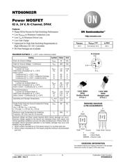
NTD60N02R
Power MOSFET
62 A, 24 V, N−Channel, DPAK
Features
• Planar HD3e Process for Fast Switching Performance
• Low R
DS(on)
to Minimize Conduction Loss
• Low C
iss
to Minimize Driver Loss
• Low Gate Charge
• Optimized for High Side Switching Requirements in
High−Efficiency DC−DC Converters
• Pb−Free Packages are Available
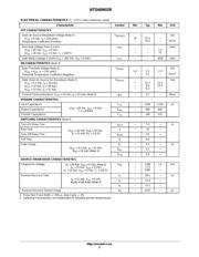
MAXIMUM RATINGS (T
J
= 25°C unless otherwise noted)
Rating
Symbol Value Unit
Drain−to−Source Voltage V
DSS
24 Vdc
Gate−to−Source Voltage − Continuous V
GS
±20 Vdc
Thermal Resistance
Junction−to−Case
Total Power Dissipation @ T
C
= 25°C
Drain Current
Continuous @ T
C
= 25°C, Chip
Continuous @ T
C
= 25°C, Limited by Package
Continuous @ T
A
= 25°C, Limited by Wires
R
JC
P
D
I
D
I
D
I
D
2.6
58
62
50
32
°C/W
W
A
A
A
Thermal Resistance
Junction−to−Ambient (Note 1)
Total Power Dissipation @ T
A
= 25°C
Drain Current − Continuous @ T
A
= 25°C
R
JA
P
D
I
D
80
1.87
10.5
C/W
W
A
Thermal Resistance
Junction−to−Ambient (Note 2)
Total Power Dissipation @ T
A
= 25°C
Drain Current − Continuous @ T
A
= 25°C
R
JA
P
D
I
D
120
1.25
8.5
°C/W
W
A
Operating and Storage Temperature T
J
, and
T
stg
−55 to
175
°C
Single Pulse Drain−to−Source Avalanche Energy
− Starting T
J
= 25°C
(V
DD
= 50 Vdc, V
GS
= 10.0 Vdc,
I
L
= 11 Apk, L = 1.0 mH, R
G
= 25 )
E
AS
60 mJ
Maximum Lead Temperature for Soldering
Purposes, 1/8″ from case for 10 seconds
T
L
260 °C
Maximum ratings are those values beyond which device damage can occur.
Maximum ratings applied to the device are individual stress limit values (not
normal operating conditions) and are not valid simultaneously. If these limits are
exceeded, device functional operation is not implied, damage may occur and
reliability may be affected.
1. When surface mounted to an FR4 board using 0.5 in sq drain pad size.
2. When surface mounted to an FR4 board using the minimum recommended
pad size.
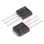
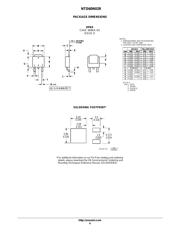
CASE 369AA
DPAK
(Surface Mount)
STYLE 2
MARKING DIAGRAM
& PIN ASSIGNMENTS
1
2
3
4
http://onsemi.com
Y = Year
WW = Work Week
60N02R = Device Code
24 V 8.4 m @ 10 V
R
DS(on)
TYP
62 A
I
D
MAXV
(BR)DSS
CASE 369D
DPAK
(Straight Lead)
STYLE 2
1
Gate
3
Source
2
Drain
4
Drain
YWW
T60
N02R
YWW
T60
N02R
1
Gate
3
Source
2
Drain
4
Drain
1
2
3
4
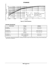
See detailed ordering and shipping information in the package
dimensions section on page 5 of this data sheet.
ORDERING INFORMATION
N−Channel
D
S
G
Verzeichnis