
herunterladen
Semiconductor Components Industries, LLC, 2011
November, 2011 − Rev. 2
1 Publication Order Number:
NSS40301MZ4/D
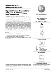
NSS40301MZ4,
NSV40301MZ4T1G
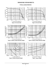
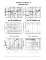
Bipolar Power Transistors
40 V, 3.0 A, Low V
CE(sat)
NPN Transistor
ON Semiconductor’s e
2
PowerEdge family of low V
CE(sat)
transistors are surface mount devices featuring ultra low saturation
voltage (V
CE(sat)
) and high current gain capability. These are designed
for use in low voltage, high speed switching applications where
affordable efficient energy control is important.
Typical applications are DC−DC converters and power management
in portable and battery powered products such as cellular and cordless
phones, PDAs, computers, printers, digital cameras and MP3 players.
Other applications are low voltage motor controls in mass storage
products such as disc drives and tape drives. In the automotive
industry they can be used in air bag deployment and in the instrument
cluster. The high current gain allows e
2
PowerEdge devices to be
driven directly from PMU’s control outputs, and the Linear Gain
(Beta) makes them ideal components in analog amplifiers.
Features
AEC−Q101 Qualified and PPAP Capable
NSV Prefix for Automotive and Other Applications Requiring
Unique Site and Control Change Requirements
These Devices are Pb−Free, Halogen Free/BFR Free and are RoHS
Compliant*
*For additional information on our Pb−Free strategy and soldering details, please
download the ON Semiconductor Soldering and Mounting Techniques
Reference Manual, SOLDERRM/D.
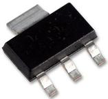
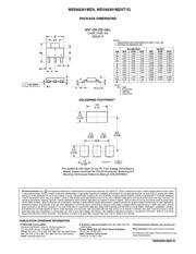
SOT−223
CASE 318E
STYLE 1
MARKING DIAGRAM
Schematic
C 2, 4
B 1 E 3
Top View Pinout
C
CEB
4
123
NPN TRANSISTOR
3.0 AMPERES
40 VOLTS, 2.0 WATTS
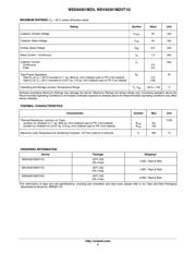
See detailed ordering and shipping information in the package
dimensions section on page 2 of this data sheet.
ORDERING INFORMATION
PIN ASSIGNMENT
http://onsemi.com
1
40301G
AYW
A = Assembly Location
Y Year
W = Work Week
40301 = Specific Device Code
G = Pb−Free Package
Verzeichnis
- ・ Konfiguration des Pinbelegungsdiagramms on Seite 1
- ・ Abmessungen des Paketumrisses on Seite 6
- ・ Paket-Footprint-Pad-Layout on Seite 6
- ・ Teilenummerierungssystem on Seite 1 Seite 2 Seite 6
- ・ Markierungsinformationen on Seite 1
- ・ Blockdiagramm on Seite 1
- ・ Typisches Anwendungsschaltbild on Seite 1
- ・ Technische Daten on Seite 2
- ・ Anwendungsbereich on Seite 1
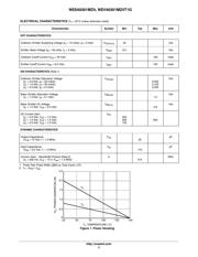
- ・ Elektrische Spezifikation on Seite 3