
herunterladen
© Semiconductor Components Industries, LLC, 2009
August, 2009 − Rev. 1
1 Publication Order Number:
NSS60200L/D
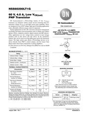
NSS60200LT1G
60 V, 4.0 A, Low V
CE(sat)
PNP Transistor
ON Semiconductor’s e
2
PowerEdge family of low V
CE(sat)
transistors are miniature surface mount devices featuring ultra low
saturation voltage (V
CE(sat)
) and high current gain capability. These
are designed for use in low voltage, high speed switching applications
where affordable efficient energy control is important.
Typical applications are DC−DC converters and power management
in portable and battery powered products such as cellular and cordless
phones, PDAs, computers, printers, digital cameras and MP3 players.
Other applications are low voltage motor controls in mass storage
products such as disc drives and tape drives. In the automotive
industry they can be used in air bag deployment and in the instrument
cluster. The high current gain allows e
2
PowerEdge devices to be
driven directly from PMU’s control outputs, and the Linear Gain
(Beta) makes them ideal components in analog amplifiers.
• These Devices are Pb−Free, Halogen Free/BFR Free and are RoHS
Compliant
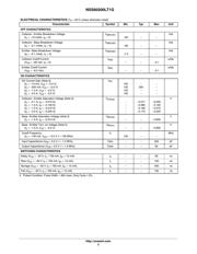
MAXIMUM RATINGS (T
A
= 25°C)
Rating Symbol Max Unit
Collector-Emitter Voltage V
CEO
−60 Vdc
Collector-Base Voltage V
CBO
−80 Vdc
Emitter-Base Voltage V
EBO
−7.0 Vdc
Collector Current − Continuous I
C
−2.0 A
Collector Current − Peak I
CM
−4.0 A
THERMAL CHARACTERISTICS
Characteristic Symbol Max Unit
Total Device Dissipation
T
A
= 25°C
Derate above 25°C
P
D
(Note 1) 460
3.7
mW
mW/°C
Thermal Resistance,
Junction−to−Ambient
R
q
JA
(Note 1)
270 °C/W
Total Device Dissipation
T
A
= 25°C
Derate above 25°C
P
D
(Note 2) 540
4.3
mW
mW/°C
Thermal Resistance,
Junction−to−Ambient
R
q
JA
(Note 2)
230 °C/W
Junction and Storage
Temperature Range
T
J
, T
stg
−55 to
+150
°C
Stresses exceeding Maximum Ratings may damage the device. Maximum
Ratings are stress ratings only. Functional operation above the Recommended
Operating Conditions is not implied. Extended exposure to stresses above the
Recommended Operating Conditions may affect device reliability.
1. FR−4 @ 100 mm
2
, 1 oz. copper traces.
2. FR−4 @ 500 mm
2
, 1 oz. copper traces.
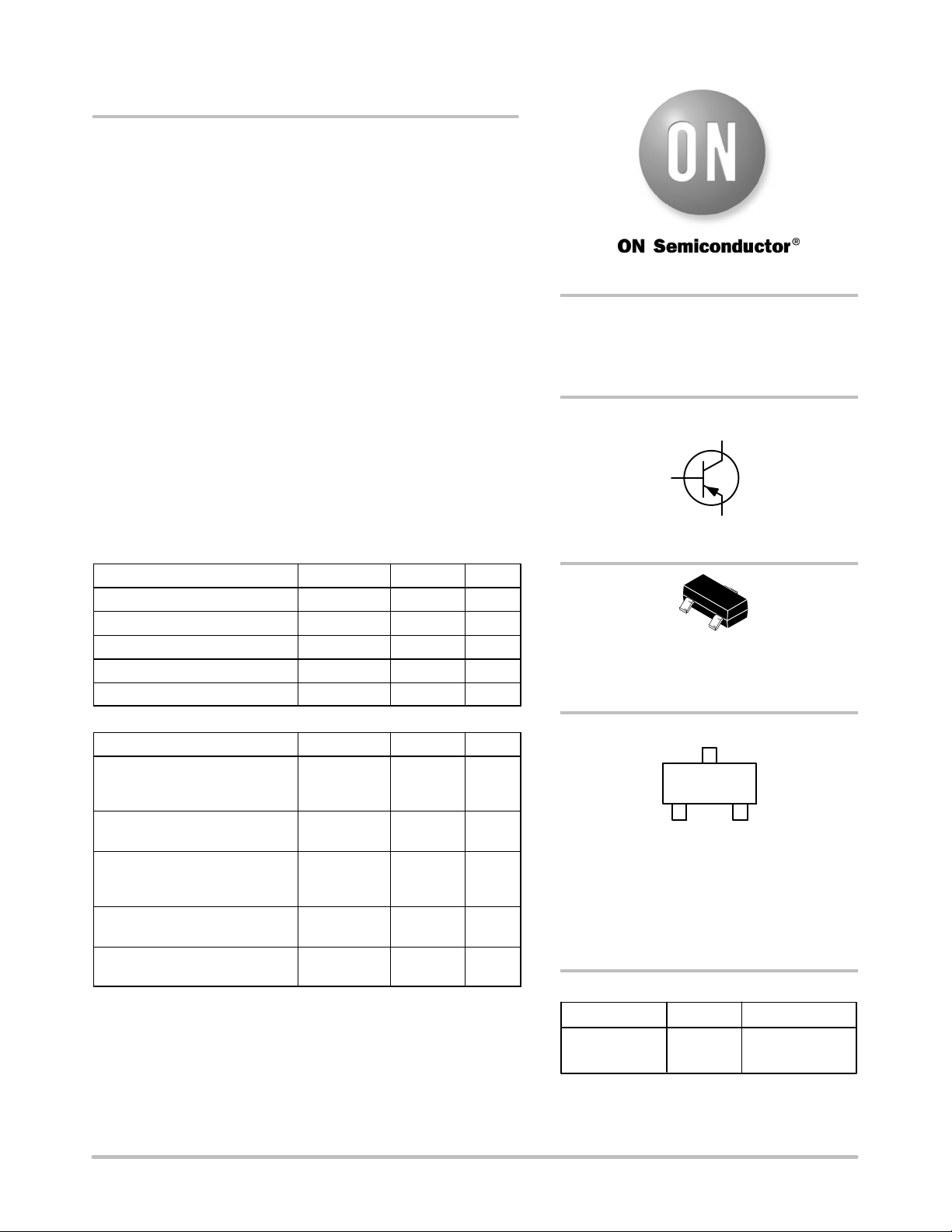
Device Package Shipping
†
ORDERING INFORMATION
NSS60200LT1G SOT−23
(Pb−Free)
3000/Tape & Reel
MARKING DIAGRAM
COLLECTOR
3
1
BASE
2
EMITTER
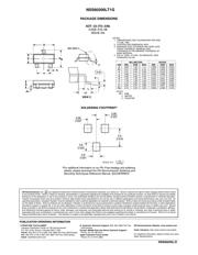
SOT−23 (TO−236)
CASE 318
STYLE 6
3
2
1
http://onsemi.com
−60 VOLTS, 4.0 AMPS
PNP LOW V
CE(sat)
TRANSISTOR
EQUIVALENT R
DS(on)
80 mW
†For information on tape and reel specifications,
including part orientation and tape sizes, please
refer to our Tape and Reel Packaging Specification
Brochure, BRD8011/D.
1
VG MG
G
VG = Specific Device Code
M = Date Code*
G = Pb−Free Package
*Date Code orientation and/or overbar may
vary depending upon manufacturing location.
(Note: Microdot may be in either location)
Verzeichnis