
herunterladen
© Semiconductor Components Industries, LLC, 2014
August, 2014 − Rev. 11
1 Publication Order Number:
MC14040B/D
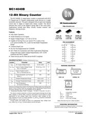
MC14040B
12-Bit Binary Counter
The MC14040B 12−stage binary counter is constructed with MOS
P−Channel and N−Channel enhancement mode devices in a single
monolithic structure. This part is designed with an input wave shaping
circuit and 12 stages of ripple−carry binary counter. The device
advances the count on the negative−going edge of the clock pulse.
Applications include time delay circuits, counter controls, and
frequency−driving circuits.
Features
• Fully Static Operation
• Diode Protection on All Inputs
• Supply Voltage Range = 3.0 Vdc to 18 Vdc
• Capable of Driving Two Low−power TTL Loads or One
Low−power Schottky TTL Load Over the Rated Temperature
Range
• Common Reset Line
• Pin−for−Pin Replacement for CD4040B
• NLV Prefix for Automotive and Other Applications Requiring
Unique Site and Control Change Requirements; AEC−Q100
Qualified and PPAP Capable
• These Devices are Pb−Free and are RoHS Compliant
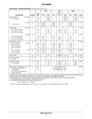
MAXIMUM RATINGS (Voltages Referenced to V
SS
)
Symbol
Parameter Value Unit
V
DD
DC Supply Voltage Range −0.5 to +18.0 V
V
in
, V
out
Input or Output Voltage Range
(DC or Transient)
−0.5 to V
DD
+ 0.5 V
I
in
, I
out
Input or Output Current
(DC or Transient) per Pin
±10 mA
P
D
Power Dissipation, per Package
(Note 1)
500 mW
T
A
Ambient Temperature Range −55 to +125 °C
T
stg
Storage Temperature Range −65 to +150 °C
T
L
Lead Temperature
(8−Second Soldering)
260 °C
Stresses exceeding those listed in the Maximum Ratings table may damage the
device. If any of these limits are exceeded, device functionality should not be
assumed, damage may occur and reliability may be affected.
1. Temperature Derating: “D/DW” Packages: –7.0 mW/_C From 65_C To 125_C
This device contains protection circuitry to guard against damage due to high
static voltages or electric fields. However, precautions must be taken to avoid
applications of any voltage higher than maximum rated voltages to this
high−impedance circuit. For proper operation, V
in
and V
out
should be constrained
to the range V
SS
≤ (V
in
or V
out
) ≤ V
DD
.
Unused inputs must always be tied to an appropriate logic voltage level
(e.g., either V
SS
or V
DD
). Unused outputs must be left open.
http://onsemi.com
MARKING DIAGRAMS
SOIC−16
TSSOP−16
14040BG
AWLYWW
SOEIAJ−16
MC14040B
ALYWG
See detailed ordering and shipping information in the package
dimensions section on page 2 of this data sheet.
ORDERING INFORMATION
1
16
1
16
14
040B
ALYW G
G
1
16
A = Assembly Location
WL, L = Wafer Lot
YY, Y = Year
WW, W = Work Week
G or G = Pb−Free Package
(Note: Microdot may be in either location)
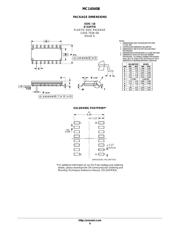
SOIC−16
D SUFFIX
CASE 751B
TSSOP−16
DT SUFFIX
CASE 948F
SOEIAJ−16
F SUFFIX
CASE 966
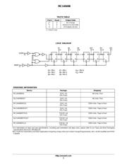
PIN ASSIGNMENT
13
14
15
16
9
10
11
125
4
3
2
1
8
7
6
Q9
Q8
Q10
Q11
V
DD
Q1
C
R
Q7
Q5
Q6
Q12
V
SS
Q2
Q3
Q4
Verzeichnis
- ・ Konfiguration des Pinbelegungsdiagramms on Seite 1
- ・ Abmessungen des Paketumrisses on Seite 6 Seite 7 Seite 8
- ・ Paket-Footprint-Pad-Layout on Seite 6 Seite 7
- ・ Teilenummerierungssystem on Seite 1 Seite 2 Seite 8
- ・ Markierungsinformationen on Seite 1 Seite 8
- ・ Typisches Anwendungsschaltbild on Seite 2
- ・ Technische Daten on Seite 2
- ・ Anwendungsbereich on Seite 1 Seite 2 Seite 5
- ・ Elektrische Spezifikation on Seite 3
- ・ Teilenummernliste on Seite 1