
herunterladen

© Semiconductor Components Industries, LLC, 2006
April, 2006 − Rev. 7
1 Publication Order Number:
NL27WZ14/D
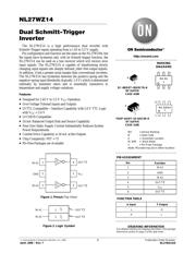
NL27WZ14
Dual Schmitt−Trigger
Inverter
The NL27WZ14 is a high performance dual inverter with
Schmitt−Trigger inputs operating from a 1.65 to 5.5 V supply.
Pin configuration and function are the same as the NL27WZ04, but
the inputs have hysteresis and, with its Schmitt trigger function, the
NL27WZ14 can be used as a line receiver which will receive slow
input signals. The NL27WZ14 is capable of transforming slowly
changing input signals into sharply defined, jitter−free output signals.
In addition, it has a greater noise margin than conventional inverters.
The NL27WZ14 has hysteresis between the positive−going and the
negative−going input thresholds (typically 1.0 V) which is determined
internally by transistor ratios and is essentially insensitive to
temperature and supply voltage variations.
Features
• Designed for 1.65 V to 5.5 V V
CC
Operation
• Over Voltage Tolerant Inputs and Outputs
• LVTTL Compatible − Interface Capability with 5.0 V TTL Logic
with V
CC
= 3.0 V
• LVCMOS Compatible
• 24 mA Balanced Output Sink and Source Capability
• Near Zero Static Supply Current Substantially Reduces System
Power Requirements
• Current Drive Capability is 24 mA at the Outputs
• Chip Complexity: FET = 72
• Pb−Free Packages are Available
V
CC
IN A1
OUT Y1
GND
IN A2
OUT Y2
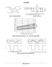
Figure 1. Pinout (Top View)
Figure 2. Logic Symbol
IN A2
OUT Y2
OUT Y1IN A1
1
2
3
6
5
4
1
1
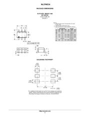
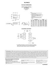
http://onsemi.com
MARKING
DIAGRAMS
MA = Device Marking
M = Date Code
A = Assembly Location
W, WW = Work Week
G = Pb−Free Package
(Note: Microdot may be in either location)
SC−88/SOT−363/SC70−6
DF SUFFIX
CASE 419B
TSOP−6/SOT−23−6/SC59−6
DT SUFFIX
CASE 318G
1
6
1
6
1
6
MA AWWG
G
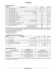
See detailed ordering and shipping information in the package
dimensions section on page 2 of this data sheet.
ORDERING INFORMATION
PIN ASSIGNMENT
1
2
3IN A2
IN A1
GND
4
5V
CC
OUT Y2
Pin
Function
FUNCTION TABLE
L
A Input Y Output
H
HL
6 OUT Y1
MA MG
G
Verzeichnis
- ・ Konfiguration des Pinbelegungsdiagramms on Seite 1
- ・ Abmessungen des Paketumrisses on Seite 5 Seite 6
- ・ Paket-Footprint-Pad-Layout on Seite 5 Seite 6
- ・ Teilenummerierungssystem on Seite 1 Seite 2 Seite 6
- ・ Markierungsinformationen on Seite 1
- ・ Technische Daten on Seite 2
- ・ Anwendungsbereich on Seite 4
- ・ Elektrische Spezifikation on Seite 3