
herunterladen
Semiconductor Components Industries, LLC, 2005
January, 2005 − Rev. 3
1 Publication Order Number:
NL17SZ02/D
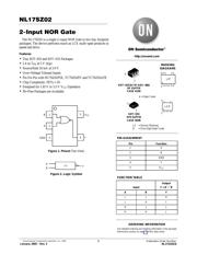
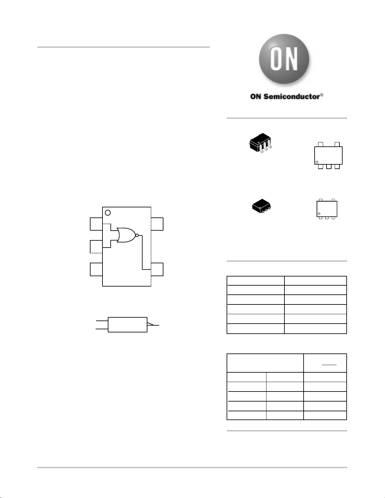
NL17SZ02
2−Input NOR Gate
The NL17SZ02 is a single 2−input NOR Gate in two tiny footprint
packages. The device performs much as LCX multi−gate products in
speed and drive.
Features
• Tiny SOT−353 and SOT−553 Packages
• 2.4 ns T
PD
at 5 V (typ)
• Source/Sink 24 mA at 3.0 V
• Over−Voltage Tolerant Inputs
• Pin For Pin with NC7SZ02P5X, TC7SZ02FU and TC7SZ02AFE
• Chip Complexity: FETs = 20
• Designed for 1.65 V to 5.5 V V
CC
Operation
• Pb−Free Packages are Available
Figure 1. Pinout (Top View)
Figure 2. Logic Symbol
1
Y
A
B
V
CC
B
A
1
2
3
5
4
GND
Y
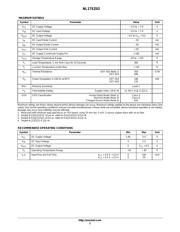
See detailed ordering and shipping information in the package
dimensions section on page 4 of this data sheet.
ORDERING INFORMATION
MARKING
DIAGRAMS
d = Date Code
L3
d
SOT−553
XV5 SUFFIX
CASE 463B
L3 = Device Marking
D = One Digit Date Code
L3 D
SOT−353/SC70−5/SC−88A
DF SUFFIX
CASE 419A
1
5
PIN ASSIGNMENT
Pin
1
2
3
4
5
Function
A
B
GND
Y
V
CC
Input
FUNCTION TABLE
B
L
H
L
H
Output
Y = A
B
Y
H
L
L
L
A
L
L
H
H
1
5
1
5
1
5
http://onsemi.com
Verzeichnis
- ・ Konfiguration des Pinbelegungsdiagramms on Seite 1
- ・ Abmessungen des Paketumrisses on Seite 5 Seite 6
- ・ Paket-Footprint-Pad-Layout on Seite 5 Seite 6
- ・ Teilenummerierungssystem on Seite 1 Seite 4 Seite 6
- ・ Markierungsinformationen on Seite 1
- ・ Technische Daten on Seite 4
- ・ Elektrische Spezifikation on Seite 3