
herunterladen
July 2002
2002 Fairchild Semiconductor Corporation
NDS0610 Rev B(W)
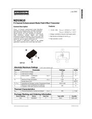
NDS0610
P-Channel Enhancement Mode Field Effect Transistor
General Description
These P-Channel enhancement mode field effect
transistors are produced using Fairchild’s proprietary,
high cell density, DMOS technology. This very high
density process has been designed to minimize on-
state resistance, provide rugged and reliable
performance and fast switching. They can be used, with
a minimum of effort, in most applications requiring up to
120mA DC and can deliver current up to 1A.
This product is particularly suited to low voltage
applications requiring a low current high side switch.
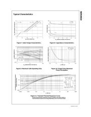
Features
• −0.12A, −60V. R
DS(ON)
= 10 Ω @ V
GS
= −10 V
R
DS(ON)
= 20 Ω @ V
GS
= −4.5 V
• Voltage controlled p-channel small signal switch
• High density cell design for low R
DS(ON)
• High saturation current
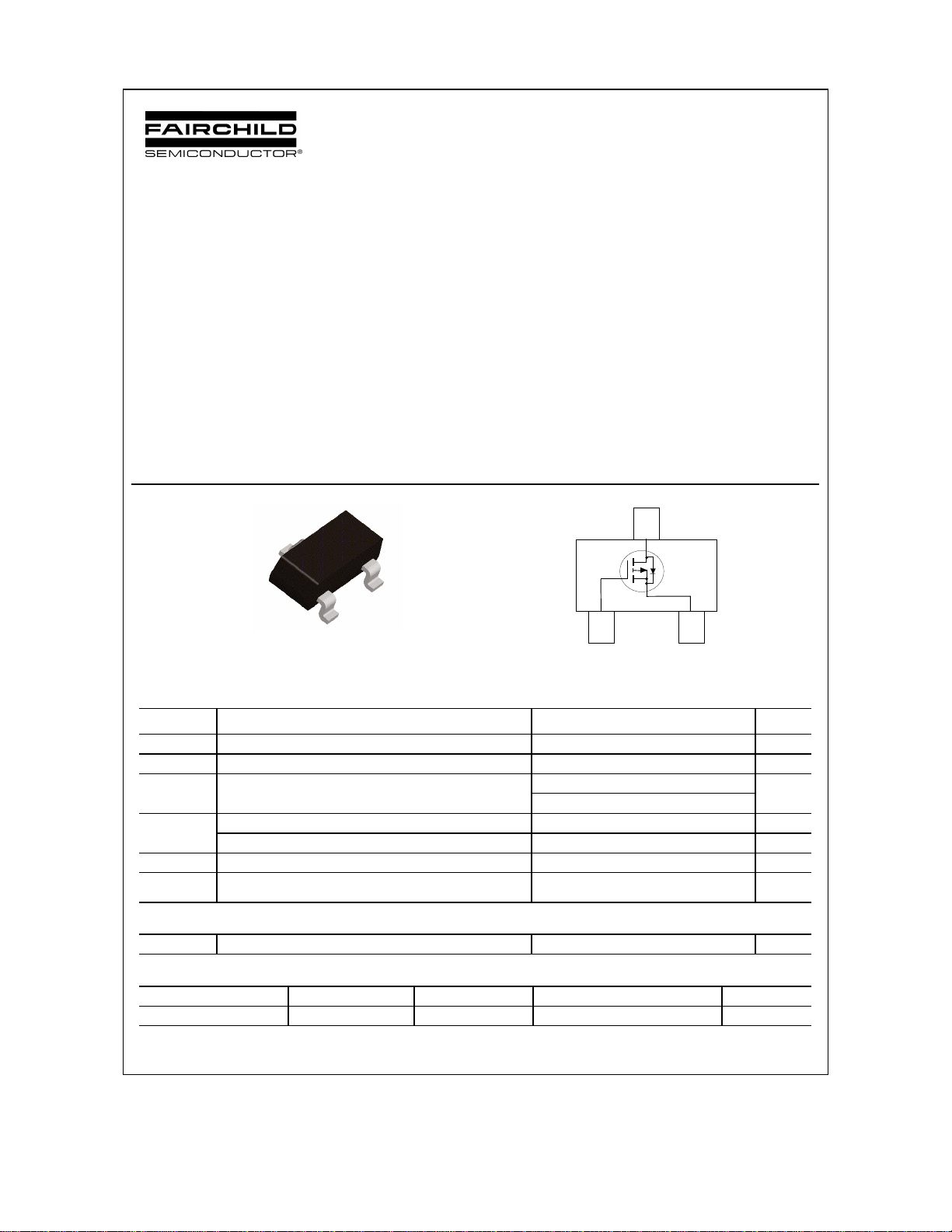
G
D
S
SOT-23
D
SG
Absolute Maximum Ratings T
A
=25
o
C unless otherwise noted
Symbol Parameter Ratings Units
V
DSS
Drain-Source Voltage
−60
V
V
GSS
Gate-Source Voltage
±20
V
I
D
Drain Current – Continuous (Note 1)
−0.12
A
– Pulsed
−1
Maximum Power Dissipation (Note 1) 0.36
W
P
D
Derate Above 25°C
2.9
mW/°C
T
J
, T
STG
Operating and Storage Junction Temperature Range
−55 to +150 °C
T
L
Maximum Lead Temperature for Soldering
Purposes, 1/16” from Case for 10 Seconds
300
°C
Thermal Characteristics
R
θJA
Thermal Resistance, Junction-to-Ambient
(Note 1) 350
°C/W
Package Marking and Ordering Information
Device Marking Device Reel Size Tape width Quantity
610 NDS0610 7’’ 8mm 3000 units
NDS0610
Verzeichnis