
herunterladen
Semiconductor Components Industries, LLC, 2013
May, 2013 − Rev. 17
1 Publication Order Number:
NCP5661/D
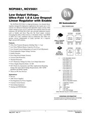
NCP5661, NCV5661
Low Output Voltage,
Ultra-Fast 1.0 A Low Dropout
Linear Regulator with Enable
The NCP5661/NCV5661 is a high performance, low dropout linear
regulator designed for high power applications that require up to 1.0 A
current. It is offered in both fixed and adjustable output versions. With
output voltages as low as 0.9 V and ultra−fast response times for load
transients, the NCP5661/NCV5661 also provides additional features
such as Enable and Error Flag (for the fixed output version),
increasing the utility of these devices. A thermally robust, 5 pin DPAK
or DFN 3x3.3 mm, combined with an architecture that offers low
ground current (independent of load), provides for a superior
high−current LDO solution.
Features
Ultra−Fast Transient Response (Settling Time: 1−3 ms)
Low Noise Without Bypass Capacitor (26 mV
rms)
Low Ground Current Independent of Load (3.0 mA Maximum)
Fixed/Adjustable Output Voltage Versions
Enable Function
Error Flag (Fixed Output Version)
Current Limit Protection
Thermal Protection
0.9 V Reference Voltage for Ultra−Low Output Operation
Power Supply Rejection Ratio > 65 dB
NCV Prefix for Automotive and Other Applications Requiring
Unique Site and Control Change Requirements; AEC−Q100
Qualified and PPAP Capable
These are Pb−Free Devices
Applications
Servers
ASIC Power Supplies
Post Regulation for Power Supplies
Constant Current Source
Networking Equipment
Gaming and STB Modules
DPAK−5 CENTER
LEAD CROP
CASE 175AA
1
5
MARKING
DIAGRAMS
http://onsemi.com
See detailed ordering and shipping information in the package
dimensions section on page 10 of this data sheet.
ORDERING INFORMATION
5661xG
ALYWW
x = A for Adjustable Version
B for Fixed 1.2 V
C for Fixed 3.3 V
D for Fixed 1.5 V
E for Fixed 1.8 V
F for Fixed 2.5 V
G for Fixed 2.8 V
H for Fixed 3.0 V
1
DFN6
MN SUFFIX
CASE 506AX
661x
AYWWG
G
1
V5661xG
ALYWW
V661
zzz
AYWWG
G
1
NCP5661 NCV5661
NCP5661 NCV5661
A = Assembly Location
L = Wafer Lot
Y = Year
WW = Work Week
G = Pb−Free
G = Pb−Free Package
zzz = 12 for Fixed 1.2 V
15 for Fixed 1.5 V
18 for Fixed 1.8 V
25 for Fixed 2.5 V
28 for Fixed 2.8 V
30 for Fixed 3.0 V
33 for Fixed 3.3 V
ADJ for Adjustable Version
(Note: Microdot may be in either location)
Verzeichnis
- ・ Abmessungen des Paketumrisses on Seite 11 Seite 12
- ・ Paket-Footprint-Pad-Layout on Seite 11 Seite 12
- ・ Teilenummerierungssystem on Seite 1 Seite 10 Seite 12
- ・ Markierungsinformationen on Seite 1 Seite 12
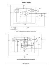
- ・ Blockdiagramm on Seite 5
- ・ Beschreibung der Funktionen on Seite 2
- ・ Technische Daten on Seite 10
- ・ Anwendungsbereich on Seite 1 Seite 10
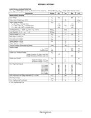
- ・ Elektrische Spezifikation on Seite 3 Seite 4