
herunterladen
Semiconductor Components Industries, LLC, 2013
April, 2013 − Rev. 12
1 Publication Order Number:
NCP5500/D
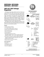
NCP5500, NCV5500,
NCP5501, NCV5501
500 mA LDO Voltage
Regulator
These linear low drop voltage regulators provide up to 500 mA over
a user−adjustable output range of 1.25 V to 5.0 V, or at a fixed output
voltage of 1.5 V, 3.3 V or 5.0 V, with typical output voltage accuracy
better than 3%. An internal PNP pass transistor permits low dropout
voltage and operation at full load current at the minimum input
voltage. NCV versions are qualified for demanding automotive
applications that require extended temperature operation and site and
change control. NCP5500 and NCV5500 versions include an
Enable/Shutdown function and are available in a DPAK 5 and SOIC 8
packages. NCP5501 and NCV5501 versions are available in DPAK 3
for applications that do not require logical on/off control.
This regulator family is ideal for applications that require a broad
input voltage range, and low dropout performance up to 500 mA load
using low cost ceramic capacitors. Integral protection features include
short circuit current and thermal shutdown.
Features
Output Current up to 500 mA
2.9% Output Voltage Accuracy
Low Dropout Voltage (230 mV at 500 mA)
Enable Control Pin (NCP5500 / NCV5500)
Reverse Bias Protection
Short Circuit Protection
Thermal Shutdown
Wide Operating Temperature Range
NCV5500 / NCV5501; −40C to +125C Ambient Temperature
NCP5500 / NCP5501; −40C to +85C Ambient Temperature
NCV Prefix for Automotive and Other Applications Requiring
Unique Site and Control Change Requirements; AEC−Q100
Qualified and PPAP Capable
Stable with Low Cost Ceramic Capacitors
These are Pb−Free Devices
Typical Applications
Automotive
Industrial and Consumer
Post SMPS Regulation
Point of Use Regulation
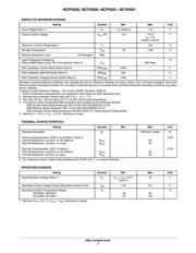
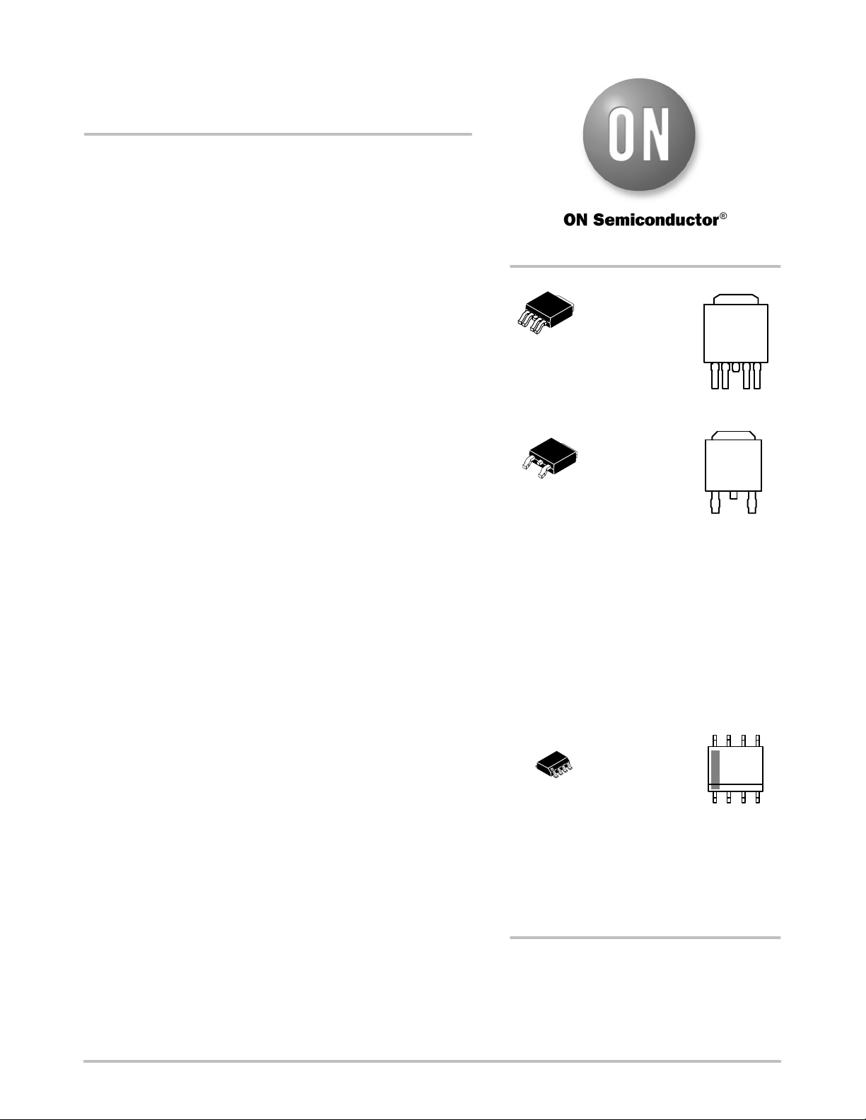
x5500yG
ALYWW
15
DPAK 5
CENTER LEAD CROP
CASE 175AA
See detailed ordering and shipping information in the package
dimensions section on page 10 of this data sheet.
ORDERING INFORMATION
MARKING DIAGRAMS
http://onsemi.com
x = P (NCP), V (NCV)
5500/1 = Device Code
y = Output Voltage
= L = 1.5 V
= T = 3.3 V
= U = 5.0 V
= W = Adjustable
A = Assembly Location
L = Wafer Lot
Y = Year
WW = Work Week
G = Pb−Free Package
1
2
3
4
DPAK 3
SINGLE GAUGE
CASE 369C
13
x5501yG
ALYWW
5
1
Pin 1. EN
2. V
in
TAB,3. GND
4. V
out
5. NC/ADJ
Pin 1. V
in
TAB,2. GND
3. V
out
5500x
ALYW
G
1
8
1
8
SOIC−8
CASE 751
Pin 1. V
in
2. GND
3. GND
4. V
out
5. NC/ADJ
6. GND
7. GND
8. EN
x = Output Voltage, NCP/NCV
A = Adjustable, NCV
B = Adjustable, NCP
A = Assembly Location
L = Wafer Lot
Y = Year
W = Work Week
G = Pb−Free Package
Verzeichnis
- ・ Konfiguration des Pinbelegungsdiagramms on Seite 2
- ・ Abmessungen des Paketumrisses on Seite 11 Seite 12 Seite 13
- ・ Paket-Footprint-Pad-Layout on Seite 11 Seite 12 Seite 13
- ・ Teilenummerierungssystem on Seite 1 Seite 10 Seite 13
- ・ Markierungsinformationen on Seite 1 Seite 10 Seite 13
- ・ Blockdiagramm on Seite 2
- ・ Typisches Anwendungsschaltbild on Seite 1 Seite 2
- ・ Beschreibung der Funktionen on Seite 2
- ・ Technische Daten on Seite 3 Seite 10
- ・ Anwendungsbereich on Seite 1 Seite 10
- ・ Elektrische Spezifikation on Seite 3 Seite 4