


herunterladen
Semiconductor Components Industries, LLC, 2000
July, 2000 – Rev. 3
1 Publication Order Number:
NCP302/D
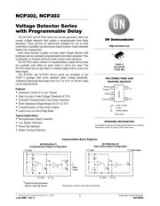
NCP302, NCP303
Voltage Detector Series
with Programmable Delay
The NCP302 and NCP303 series are second generation ultra–low
current voltage detectors that contain a programmable time delay
generator. These devices are specifically designed for use as reset
controllers in portable microprocessor based systems where extended
battery life is paramount.
Each series features a highly accurate under voltage detector with
hysteresis and an externally programmable time delay generator. This
combination of features prevents erratic system reset operation.
The NCP302 series consists of complementary output devices that
are available with either an active high or active low reset. The
NCP303 series has an open drain N–channel output with an active low
reset output.
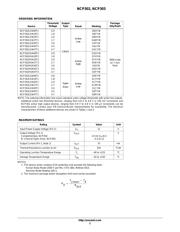
The NCP302 and NCP303 device series are available in the
TSOP–5 package with seven standard under voltage thresholds.
Additional thresholds that range from 0.9 V to 4.9 V in 100 mV steps
can be manufactured.
Features
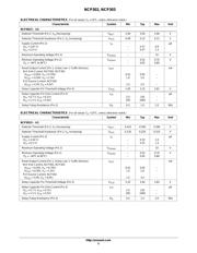
• Quiescent Current of 0.5 µA Typical
• High Accuracy Under Voltage Threshold of 2.0%
• Externally Programmable Time Delay Generator
• Wide Operating Voltage Range of 0.8 V to 10 V
• Complementary or Open Drain Output
• Active Low or Active High Reset
Typical Applications
• Microprocessor Reset Controller
• Low Battery Detection
• Power Fail Indicator
• Battery Backup Detection
Representative Block Diagrams
This device contains 28 active transistors.
NCP303LSNxxT1
Open Drain Output Configuration
NCP302xSNxxT1
Complementary Output Configuration
V
ref
2 Input
1
Reset
Output
3 Gnd
5C
D
R
D
V
ref
2 Input
3 Gnd
5C
D
R
D
1 Reset Output
* Inverter for active low devices.
* Buffer for active high devices.
*
http://onsemi.com
See detailed ordering and shipping information in the ordering
information section on page 2 of this data sheet.
ORDERING INFORMATION
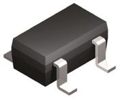
TSOP–5
SN SUFFIX
CASE 483
1
5
PIN CONNECTIONS AND
MARKING DIAGRAM
1
3
N.C.
Reset
Output
2
Input
Ground
4
C
D
5
xxxYW
(Top View)
xxx = 302 or 303
Y = Year
W = Work Week
Verzeichnis
- ・ Konfiguration des Pinbelegungsdiagramms on Seite 1
- ・ Abmessungen des Paketumrisses on Seite 17
- ・ Teilenummerierungssystem on Seite 1 Seite 2 Seite 20
- ・ Markierungsinformationen on Seite 1 Seite 2
- ・ Blockdiagramm on Seite 1
- ・ Typisches Anwendungsschaltbild on Seite 1
- ・ Anwendungsbereich on Seite 1 Seite 18
- ・ Elektrische Spezifikation on Seite 3 Seite 4 Seite 5 Seite 6