
herunterladen

© Semiconductor Components Industries, LLC, 2010
December, 2010 − Rev. 2
1 Publication Order Number:
AND8468/D
AND8468/D
A 60 W ac-dc Demonstrator
with NCP1250
Prepared by: Christophe Basso
ON Semiconductor
Housed in a tiny TSOP6 package, the NCP1250 lends
itself very well to the design of moderate to high output
power converters. Some features such as Over Power
Protection (OPP) and internal Over Voltage Protection
(OVP) make the part a component of choice for applications
where high performance and cost must be combined. This
application note demonstrates the part capabilities in a 60 W
ac−dc adapter, typical of what is needed for the high−volume
net/notebook market.
A Comprehensive Feature Set
Rather than jumping directly to the board description, it is
interesting to enumerate the various features we have
packed in this part. Generally speaking, the component
operates in peak current mode control and switches at a
constant frequency when the converter delivers its nominal
power (65 kHz or 100 kHz). When the power goes down and
hits around 20% of the nominal value, the frequency is
linearly reduced down to 26 kHz typically as the load gets
lighter. When the frequency reduction is over, the part enters
skip cycle. This function will satisfy the designers looking
for efficiency performance, especially in moderate output
loading conditions. Please note that we have introduced a
low−frequency jitter that the part keeps even when operated
in frequency foldback. It will naturally help to soften the
EMI signature even when the converter does not deliver its
full output power.
To cope with Continuous Conduction Mode (CCM)
designs, the part includes adjustable slope compensation via
the inclusion of a simple series resistance with the current
sense signal. Unlike other 6−pin devices, the level can be
nicely tweaked to adjust the compensation level to the right
value, without over or under compensating the converter as
it is often the case with fixed internal settings. Finally, a 4 ms
soft−start ensures a smooth start−up sequence and prevents
the output from overshooting.
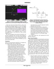
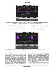
If there is one parameter that plagues most of the adapter
designs, this is the maximum authorized power that the
converter can deliver in fault condition. Beyond the
authorized value, the power supply must be stopped. When
the fault detection capitalizes on the collapsing of the
auxiliary V
CC
(as it was the case in past times), the exercise
quickly turns into a nightmare especially with a poor
coupling between the power and the auxiliary windings.
When the fault is detected by monitoring the feedback level,
as in the NCP1250 case, the situation improves. However,
the line compensation circuitry, the so−called OPP which
compensates for various propagation delays at high line,
often destroys the no−load performance as it permanently
offsets the current sense information with a portion of the
bulk (high) voltage. The NCP1250 offers a solution that will
ravish power supply designers by sensing the line input level
via the negative swing naturally present on the auxiliary
winding. Requiring two resistors only, the process is fully
non−dissipative and does not hamper the performance in
no−load conditions. Combined with the naturally−low
propagation delay of the NCP1250, the OPP performance is
excellent as confirmed by the values collected on the
prototype.
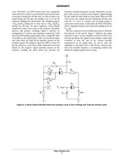
Adapters must also include some typical protections such
as Over Voltage Protection and Over Temperature
Protection (OTP). When one of these events occurs, the part
must immediately latch off. This is the case with the
NCP1250 where the latch input is easily accessible via pin
3. When activated, the device stays latched until someone
resets the converter by un−plugging the power cord. Thanks
to a simple arrangement made of one Zener diode and a
Negative Temperature Coefficient (NTC) component, the
demonstration board fully complies with the protection
requirements for most of the ac−dc adapter designs.
Finally, if controller self−supply is often a problem for
designers, this potential issue goes away with the NCP1250.
The wide V
CC
voltage range, from 9 to 28 V lets you think
of a transformer without caring too much about the auxiliary
and power windings coupling coefficient. If the leakage
inductance creates large V
CC
variations within the converter
output range, the 28 V upper V
CC
limits gives a comfortable
operating margin and will let you focus on other more
important design parameters.
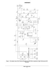
Further to this part description, it is time to explore the
demonstration board schematic.
http://onsemi.com
APPLICATION NOTE
Verzeichnis