
herunterladen
Semiconductor Components Industries, LLC, 2004
March, 2004 − Rev. 0
1 Publication Order Number:
AND8145/D
AND8145/D
A 75 W TV Power Supply
Operating in Quasi−square
Wave Resonant Mode using
the NCP1207 Controller
Prepared by: Nicolas Cyr
ON Semiconductor
Introduction
Quasi−square wave resonant converters, also known as
quasi−resonant (QR) converters, allow designing flyback
Switch−Mode Power Supplies (SMPS) with reduced
Electro−Magnetic Interference (EMI) signature and
improved efficiency. Due to the low level of generated
noise, QR SMPS are therefore very well suited to
applications dealing with RF signals, such as TVs.
ON Semiconductor NCP1207 is a QR controller that will
ease your design of an EMI−friendly TV power supply with
only a few additional components, and able to lower its
standby power down to 1.0 W.
What is Quasi−Resonance?
The term quasi−resonance is normally related to the
association of a real hard−switching converter and a
resonant tank. While the operation in terms of control is
similar to that of a standard PWM controller, an additional
network is added to shape the variables around the
MOSFET: current or voltage. Depending on the operating
mode, it becomes possible to either switch at zero current
(ZCS) or zero voltage (ZVS). Compared to a conventional
PWM converter, a QR operation offers less switching losses
but the RMS current circulating through the MOSFET
increases and forces higher conduction losses; with a careful
design, efficiency can be improved. However, one of the
main advantages in favor of the quasi−resonance is the
reduced spectrum content either conducted or radiated.
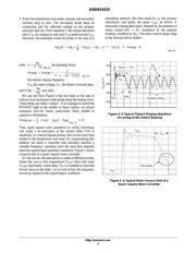
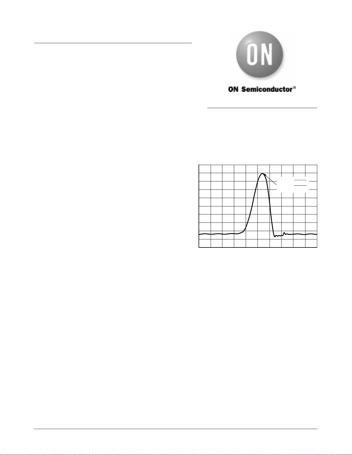
True ZVS quasi−resonance means that the voltage present
on the switch looks like a sinusoidal arch. Figure 1 shows
how such a signal could look like.
−10
50
110
170
230
Figure 1. A Truly Resonating V
DS
Signal on a
Quasi−resonant Flyback Converter
V
DS
(t) (V)
I
P
L
f
C
TOT
The main problem with this technique lies in the very high
voltage generated at the switch opening. Most of the time,
these resonant offline designs require around 1.0 kV BVdss
MOSFETs whose price is clearly incompatible with high
volume markets. As a result, designers orientate their choice
toward another compromise called quasi−square wave
resonant power supply.
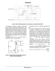
Quasi−Square Wave Resonant Converters
As we saw, true resonant operation put a constraint on
MOSFET selection by imposing a high voltage at the switch
opening. If we closely look at the standard hard−switching
waveform (Figure 2), we can see that at a given time the
drain voltage goes to a minimum. This occurs just after the
core reset.
APPLICATION NOTE
http://onsemi.com
Verzeichnis