
herunterladen
© Semiconductor Components Industries, LLC, 2007
April, 2007 − Rev. 6
1 Publication Order Number:
AND8020/D
AND8020/D
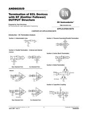
Termination of ECL Devices
with EF (Emitter Follower)
OUTPUT Structure
Prepared by: Paul Shockman
ON Semiconductor Logic Applications Engineering
CONTENTS OF APPLICATION NOTE
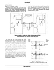
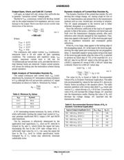
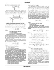
Introduction − DC Termination Analysis
Vt
R
t
R
t
R
t
R
t
R
t
R
t
Vt1
Vt2
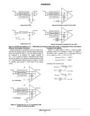
External
Internal
Near (Standard Pair) Far (Standard Pair)
Far (Standard Pair)
V
EE
R
t
R
t
R
t
R
t
R
t
Vt1
Vt2
V
EE
V
to
(Open)
V
EE
(Shorted)
V
TT
Near (Standard Pair)
V
TT
V
TT
R
E
V
EE
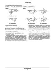
Section 2. Parallel Termination − External and Internal
Section 1. Unterminated Lines
RR
RR
Section 3. Thevenin Equivalent/Parallel Termination
R
R
Section 4. Series (Back) Termination
V
BB
V
BB
Driver
Receiver
*All Media
*
*
D1 D2
D1
D2
Section 5. Diode Termination
RR R
R
R
V
CC
V
BB
Section 6. Capacitive Coupling
R
E
R
E
R
E
R
E
R
E
R
E
R
E
R
E
Driver
APPLICATION NOTE
http://onsemi.com
Verzeichnis