
herunterladen
© Semiconductor Components Industries, LLC, 2006
April, 2006 − Rev. 0
1 Publication Order Number:
AND8215/D
AND8215/D
Semiconductor Package
Thermal Characterization
Prepared by: Roger Paul Stout, PE
ON Semiconductor
Glossary of Symbols
R(t)
JA
, R
JA
,
R
JMA
,
JA
,
JC
various notations indicating transient and
steady state thermal resistance to
ambient, case, normalized to actual
power along path of interest
JT
,
JL
, R
JS
(“junction to top”, “junction to lead”,
“junction to solder”) thermal resistance
parameter normalized to total package
power
TSP Temperature Sensitive Parameter
DUT Device Under Test
TC thermocouple
GENERAL INFORMATION
In order to measure thermal resistance of packaged
semiconductors, some basic information needs to be
provided. Die size, thickness and active area are used to
calculate certain thermal transient characteristics of the
device. Certain material properties are also necessary,
specifically density, specific heat, and thermal conductivity
of the primary materials in the package (encapsulant,
silicon, die attach, leadframe, etc.), and from these, derived
thermal transient properties of diffusivity and effusivity.
The package type is also important, surface mount or
through−hole, in order to determine mounting requirements.
Surface mount devices are tested on FR4 boards with
minimum or 1″ pad areas. TO−220 and larger power devices
are tested on a cold plate.
When measuring temperature of any power device, it is
basically impossible to put a physical thermometer onto a
device’s junction while under power. Instead, we must
utilize some temperature “sensing” method internal to the
device. For instance, in power MOSFET’s we ordinarily use
the device’s inherent “body diode.” The forward−biased
voltage drop of this pn junction has a very linear relationship
with temperature, so, when properly calibrated, we can use
it to tell us what junction temperature results from any power
condition.
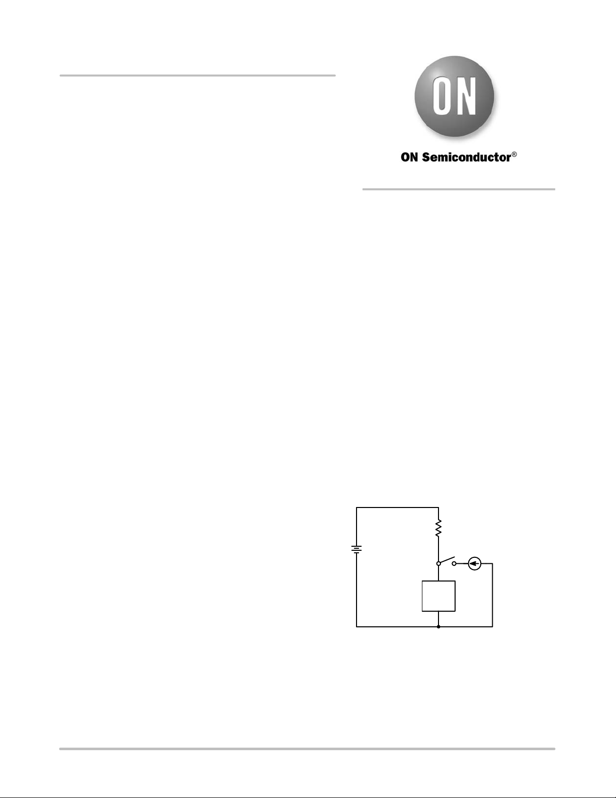
Thermal Parameter Test Procedure
The Temperature Sensitive Parameter (TSP)
To thermally characterize a semiconductor package, it is
necessary to have a temperature sensitive parameter
available (such as a diode or a resistor) within the device
being tested, which can be used to measure the die surface
temperature. The voltage of this TSP (in theory, at a fixed
current) is measured in a calibration oven at temperatures of
25, 50, 75, 100, and 125°C. The current used is very low
(typically 1.0 mA) to prevent significant self heating of the
device. (In practice, a constant current supply is
approximated by using a constant voltage supply and a large
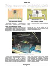
resistor in series with the TSP, as shown in Figure 1).
10.7 V
10 K
Device
under
test
Heating Power
Supply
Figure 1. Basic Thermal Test Circuit
APPLICATION NOTE
http://onsemi.com
Verzeichnis
- ・ Teilenummerierungssystem on Seite 14
- ・ Blockdiagramm on Seite 3