

herunterladen
© Semiconductor Components Industries, LLC, 2010
April, 2010 − Rev. 0
1 Publication Order Number:
AND8459/D
AND8459/D
Basics of Clock Jitter
Prepared by Baljit Chandhoke
ON Semiconductor
Introduction
This application note focuses on the different types of
clock jitter. Clock jitter is deviation of a clock edge from its
ideal location. Understanding clock jitter is very important
in applications as it plays a key role in the timing budget in
a system.
With the increasing system data rates, timing jitter has
become critical in system design, as in some instances the
system performance limit is determined by the system
timing margin. So a good understanding of the timing jitter
becomes very important in system design. Total jitter can be
separated into random jitter and deterministic jitter
components. We will not discuss the components of jitter in
this application note. We will focus on different types of
clock jitter.
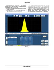
Clock timing jitter can be measured in time domain and in
frequency domain. Cycle−to−cycle jitter, period jitter and
time interval error (TIE) jitter are measured in time domain,
where as phase noise and phase jitter are measured in
frequency domain. Some of the sources of jitter are thermal
noise, power supply noise, ground bounce, PLL circuitry,
crosstalk and reflections.
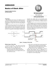
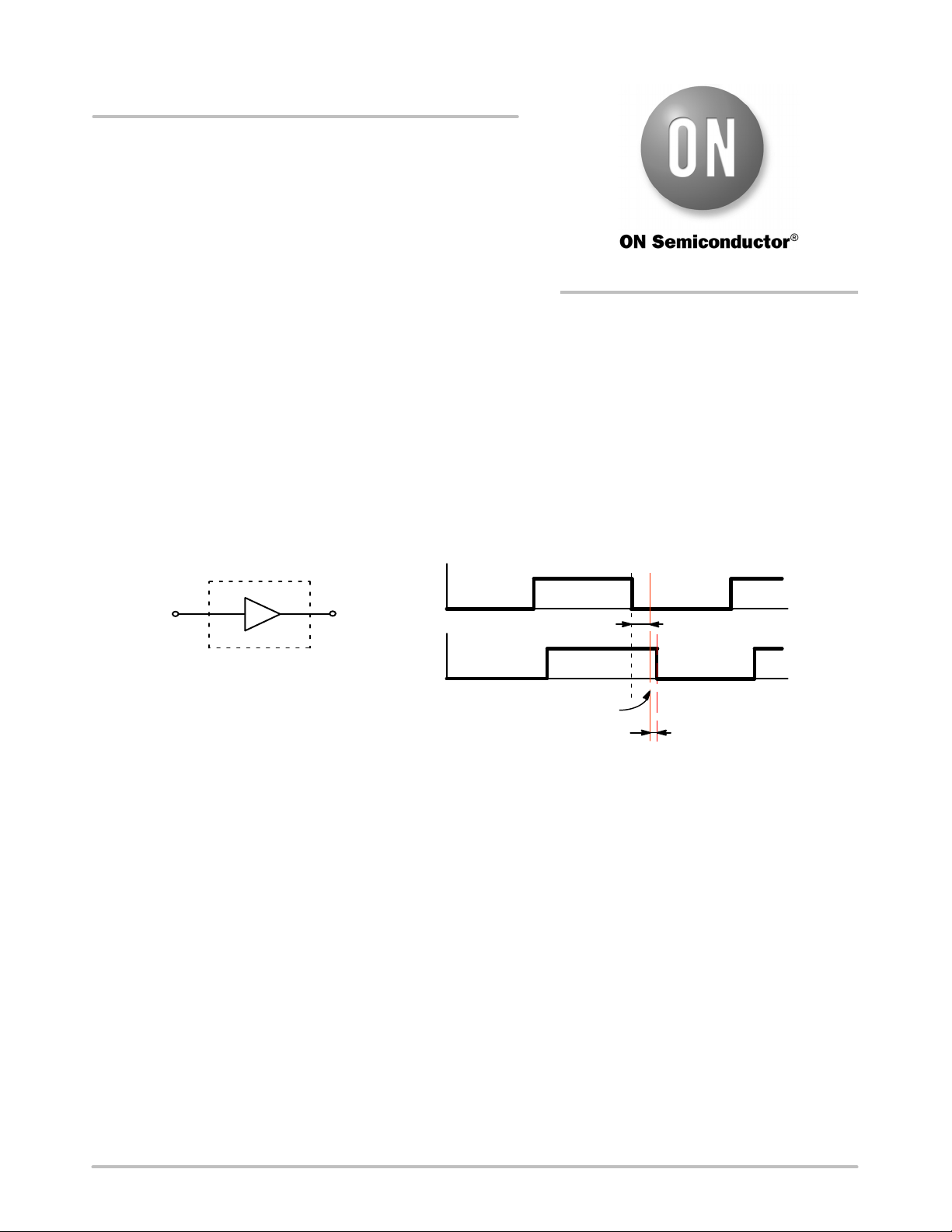
IN
A
JITTER
IN
A
The edges should
ideally be here
t
pd
Device
Figure 1. Examples of Clock Jitter
Different types of Clock Jitter
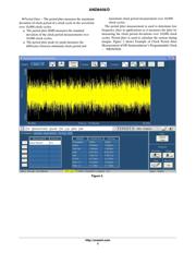
• Cycle−to−cycle Jitter − The cycle−to−cycle jitter
measures the change in clock period between any two
adjacent clock cycles over 1,000 clock cycles.
♦ The cycle−to−cycle jitter RMS measures the
standard deviation of the change in clock period
measurement between any two adjacent clock cycles
over 1,000 clock cycles.
♦ The cycle−to−cycle jitter peak−to−peak measures the
difference between minimum clock period change
and maximum clock period change between any two
adjacent clock cycles over 1,000 clock cycles.
The cycle−to−cycle jitter measurement is used to
determine high frequency jitter in applications as it
measures the jitter between two adjacent clock cycles. It is
very important to have a small value of cycle to cycle jitter
as it impacts the system timing margin.
http://onsemi.com
APPLICATION NOTE