
herunterladen
© Semiconductor Components Industries, LLC, 2013
June, 2013 − Rev. 0
1 Publication Order Number:
NB3L02/D
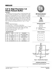
NB3L02
2.8 V, High Precision 1:2
Clock Fanout Buffer
Description
The NB3L02 is a low−skew, low jitter 1:2 clock fanout buffer, ideal
for use in portable end−equipment, such as mobile phones or tablet
applications. The MCLK_IN pin has an integrated AC coupling
capacitor and will directly accept a square or sine wave clock input,
such as a temperature compensated crystal oscillator (TCXO). The
minimum acceptable input amplitude of the sine wave is 800 mV
peak−to−peak. The NB3L02 is offered in a 0.4 mm pitch 6−ball,
wafer−level chip−scale package (WLCSP) (0.77 mm x 1.17 mm).
Features
• 800 mV Single Ended Outputs
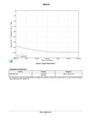
• Low Phase Noise: −144 dbc/Hz @ 10 kHz Offset
• Ultra Small Package: 0.4 mm Pitch WLCSP6 (0.77 mm x 1.17 mm)
• Exceeds JEDEC ESD Standards: 4000 V HBM, 200 V MM
• Industrial Temperature Range: −40°C to +85°C
• These are Pb−Free Devices
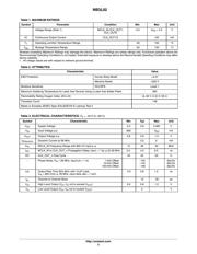
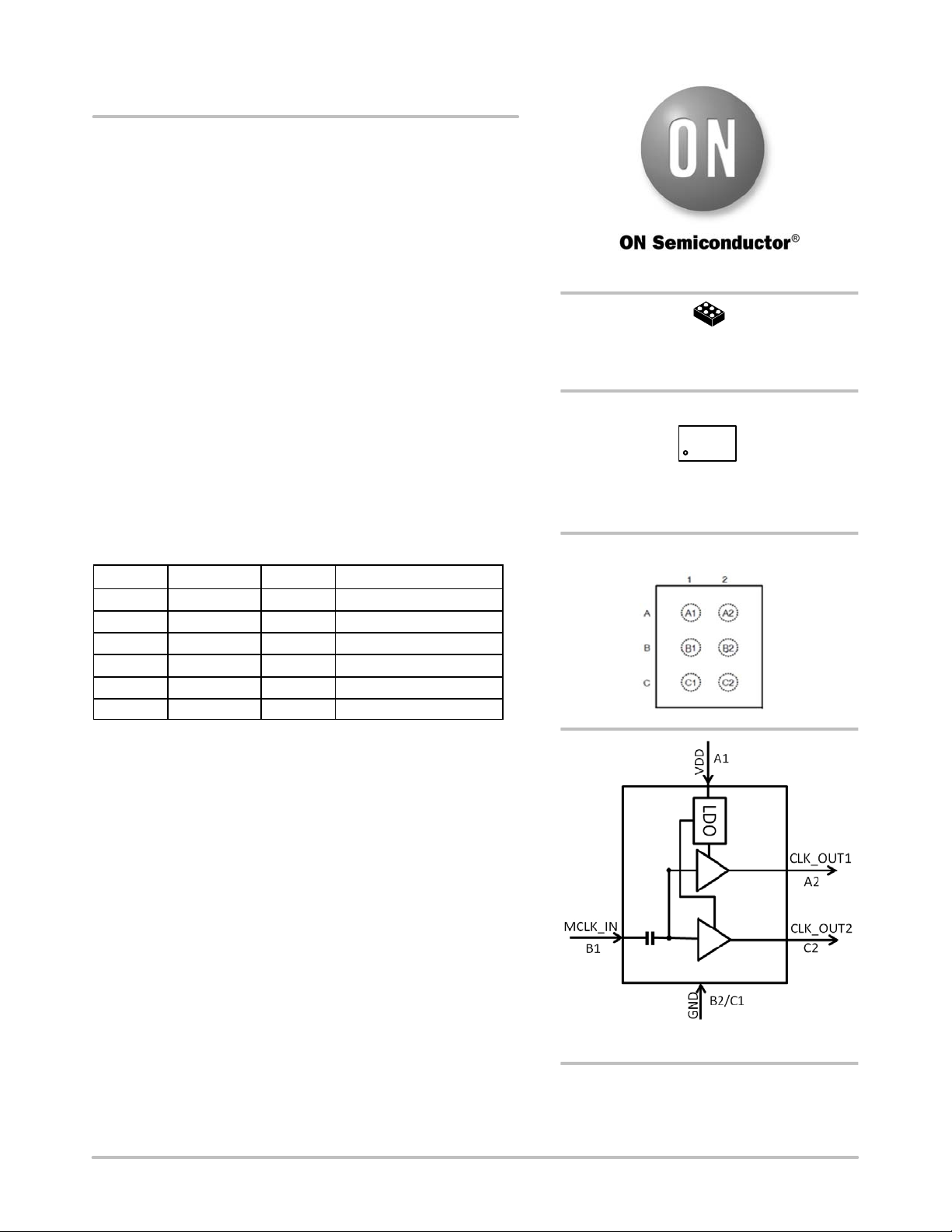
PIN DESCRIPTIONS
Ball No. Name I/O Description
A1 V
DD
I Power Supply Voltage
A2 CLK_OUT1 O Clock Output 1
B1 MCLK_IN I Master Clock Input
B2 GND − Ground
C1 GND − Ground
C2 CLK_OUT2 O Clock Output 2
MARKING DIAGRAM
WLCSP6
FC SUFFIX
CASE 567HJ
See detailed ordering and shipping information in the package
dimensions section on page 3 of this data sheet.
ORDERING INFORMATION
http://onsemi.com
http://onsemi.com
PINOUT DIAGRAM
L2 = Specific Device Code
M = Date Code
G = Pb−Free Package
L2MG
Figure 1. Simplified Block Diagram
Verzeichnis
- ・ Konfiguration des Pinbelegungsdiagramms on Seite 1
- ・ Abmessungen des Paketumrisses on Seite 4
- ・ Paket-Footprint-Pad-Layout on Seite 4
- ・ Teilenummerierungssystem on Seite 1 Seite 3 Seite 4
- ・ Markierungsinformationen on Seite 1 Seite 4
- ・ Blockdiagramm on Seite 1
- ・ Technische Daten on Seite 3
- ・ Elektrische Spezifikation on Seite 2