
herunterladen
MRFE6VP100HR5 MRFE6VP100HSR5
1
RF Device Data
Freescale Semiconductor, Inc.
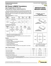
RF Power LDMOS Transistors
High Ruggedness N--Channel
Enhancement--Mode Lateral MOSFETs
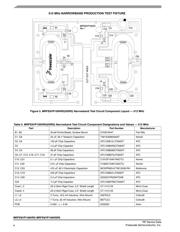
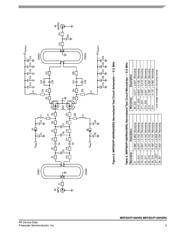
RF power transistors designed for both narrowband and broadband ISM,
broadcast and aerospace applic ations operating at frequencies f rom 1.8 to
2000 MHz. These devices are fabricated using Freescale’s enhanced
ruggedness platform and are suitable for use in applications where high VSWRs
are encountered.
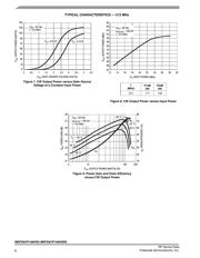
Typical Performance:
V
DD
=50Volts
Frequency
(MHz)
Signal Type
P
out
(W)
G
ps
(dB)
η
D
(%)
IMD
(dBc)
30--512
(1,3)
Two--Tone
(100 kHz spacing)
100 PEP 19.0 30.0 -- 3 0
512
(2)
CW 100 27.2 70.0 —
512
(2)
Pulse (200 μsec, 20%
Duty Cycle)
100 Peak 26.0 70.0 —
Load Mismatch/Ruggedness
Frequency
(MHz)
Signal Type VSWR
P
out
(W)
Test
Voltage
Result
512
(2)
Pulse
(100 μsec, 20%
Duty Cycle)
>65:1
at all Phase
Angles
130
(3 dB
Overdrive)
50 No Device
Degradation
512
(2)
CW 126
(3 dB
Overdrive)
1. Measured in 30--512 MHz broadband reference circuit.
2. Measured in 512 MHz narrowband test circuit.
3. The values shown are the minimum measured performance numbers across the
indicated frequency range.
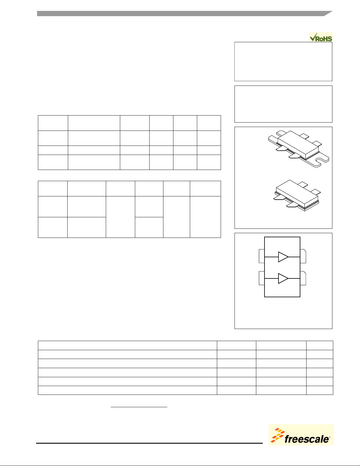
Features
• Wide Operating Frequency Range
• Extremely Rugged
• Unmatched, Capable of Very Broadband Operation
• Integrated Stability Enhancements
• Low Thermal Resistance
• Integrated ESD Protection Circuitry
• In Tape and Reel. R5 Suffix = 50 Units, 56 mm Tape Width, 13 inch Reel.
Table 1. Maximum Ratings
Rating Symbol Value Unit
Drain--Source Voltage V
DSS
--0.5, +133 Vdc
Gate--Source Voltage V
GS
--6.0, +10 Vdc
Storage Temperature Range T
stg
--65 to +150 °C
Case Operating Temperature T
C
--40 to +150 °C
Operating Junction Temperature
(4,5)
T
J
--40 to +225 °C
4. Continuous use at maximum temperature will affect MTTF.
5. MTTF calculator available at http://www.freescale.com/rf
. Select Software & Tools/Development Tools/Calculators to access MTTF
calculators by product.
Document Number: MRFE6VP100H
Rev. 0, 5/2012
Freescale Semiconductor
Technical Data
1.8--2000 MHz, 100 W, 50 V
BROADBAND
RF POWER LDMOS TRANSISTORS
MRFE6VP100HR5
MRFE6VP100HSR5
NI--780S--4
MRFE6VP100HSR5
N I -- 7 8 0 -- 4
MRFE6VP100HR5
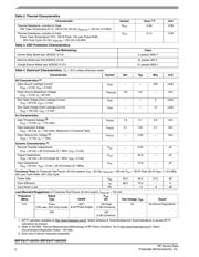
Figure 1. Pin Connections
(Top View)
Drain A
Drain B
Gate A
Gate B
Note: The backside of the package is the
source terminal for the transistor.
© Freescale Semiconductor, Inc., 2012.
A
ll rights reserved.
Verzeichnis