
herunterladen
Semiconductor Components Industries, LLC, 2001
November, 2001 – Rev. 3
Publication Order Number:
MMUN2211LT1/D
1
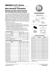
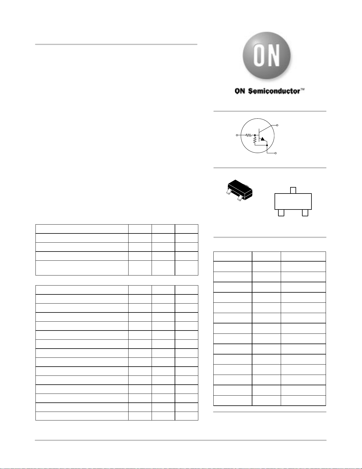
MMUN2211LT1 Series
Preferred Devices
Bias Resistor Transistor
NPN Silicon Surface Mount Transistor
with Monolithic Bias Resistor Network
This new series of digital transistors is designed to replace a single
device and its external resistor bias network. The BRT (Bias Resistor
Transistor) contains a single transistor with a monolithic bias network
consisting of two resistors; a series base resistor and a base-emitter
resistor. The BRT eliminates these individual components by
integrating them into a single device. The use of a BRT can reduce
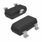
both system cost and board space. The device is housed in the SOT-23
package which is designed for low power surface mount applications.
• Simplifies Circuit Design
• Reduces Board Space and Component Count
• The SOT-23 package can be soldered using wave or reflow. The
modified gull-winged leads absorb thermal stress during soldering
eliminating the possibility of damage to the die.
• Available in 8 mm embossed tape and reel. Use the Device
Number to order the 7 inch/3000 unit reel. Replace “T1” with
“T3” in the Device Number to order the13 inch/10,000 unit reel.
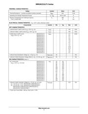
MAXIMUM RATINGS (T
A
= 25°C unless otherwise noted)
Rating
Symbol Value Unit
Collector-Base Voltage V
CBO
50 Vdc
Collector-Emitter Voltage V
CEO
50 Vdc
Collector Current I
C
100 mAdc
Total Power Dissipation @ T
A
= 25°C
(Note 1.) Derate above 25°C
P
D
*200
1.6
mW
mW/°C
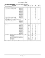
DEVICE MARKING AND RESISTOR VALUES
Device Marking R1(K) R2(K)
MMUN2211LT1 A8A 10 10
MMUN2212LT1 A8B 22 22
MMUN2213LT1 A8C 47 47
MMUN2214LT1 A8D 10 47
MMUN2215LT1 A8E 10 ∞
MMUN2216LT1 A8F 4.7 ∞
MMUN2230LT1 A8G 1.0 1.0
MMUN2231LT1 A8H 2.2 2.2
MMUN2232LT1 A8J 4.7 4.7
MMUN2233LT1 A8K 4.7 47
MMUN2234LT1 A8L 22 47
MMUN2235LT1 A8M 2.2 47
MMUN2238LT1 A8R 2.2 ∞
MMUN2241LT1 A8U 100 ∞
1. Device mounted on a FR-4 glass epoxy printed circuit board using the
minimum recommended footprint.
http://onsemi.com
SOT–23
CASE 318
STYLE 6
MARKING DIAGRAM
A8x = Device Code
x = (See Table)
PIN 3
COLLECTOR
(OUTPUT)
PIN 2
EMITTER
(GROUND)
PIN 1
BASE
(INPUT)
R1
R2
1
2
3
12
3
A8x
Preferred devices are recommended choices for future use
and best overall value.
Device Package Shipping
ORDERING INFORMATION
MMUN2211LT1 SOT–23 3000/Tape & Reel
MMUN2212LT1 SOT–23
3000/Tape & Reel
MMUN2213LT1 SOT–23 3000/Tape & Reel
MMUN2214LT1 SOT–23
3000/Tape & Reel
MMUN2215LT1 SOT–23 3000/Tape & Reel
MMUN2216LT1 SOT–23
3000/Tape & Reel
MMUN2230LT1 SOT–23 3000/Tape & Reel
MMUN2231LT1 SOT–23
3000/Tape & Reel
MMUN2232LT1 SOT–23 3000/Tape & Reel
MMUN2233LT1 SOT–23
3000/Tape & Reel
MMUN2234LT1 SOT–23 3000/Tape & Reel
MMUN2235LT1 SOT–23
3000/Tape & Reel
MMUN2238LT1 SOT–23 3000/Tape & Reel
MMUN2241LT1 SOT–23 3000/Tape & Reel
Verzeichnis