
herunterladen
© Semiconductor Components Industries, LLC, 1994
October, 2016 − Rev. 10
1 Publication Order Number:
MMBF170LT1/D
MMBF170L, NVBF170L
Power MOSFET
500 mA, 60 V, N−Channel SOT−23
Features
• NVBF Prefix for Automotive and Other Applications Requiring
Unique Site and Control Change Requirements; AEC−Q101
Qualified and PPAP Capable
• These Devices are Pb−Free and are RoHS Compliant
MAXIMUM RATINGS
Rating Symbol Value Unit
Drain−Source Voltage V
DSS
60 Vdc
Drain−Gate Voltage V
DGS
60 Vdc
Gate−Source Voltage
− Continuous
− Non−repetitive (t
p
≤ 50 ms)
V
GS
V
GSM
± 20
± 40
Vdc
Vpk
Drain Current − Continuous
− Pulsed
I
D
I
DM
0.5
0.8
Adc
THERMAL CHARACTERISTICS
Characteristic Symbol Max Unit
Total Device Dissipation FR− 5 Board
(Note 1.) T
A
= 25°C
Derate above 25°C
P
D
225
1.8
mW
mW/°C
Thermal Resistance, Junction−to−Ambient
R
q
JA
556 °C/W
Junction and Storage Temperature T
J
, T
stg
−55 to
+150
°C
Stresses exceeding those listed in the Maximum Ratings table may damage the
device. If any of these limits are exceeded, device functionality should not be
assumed, damage may occur and reliability may be affected.
1. FR−5 = 1.0 0.75 0.062 in.
3
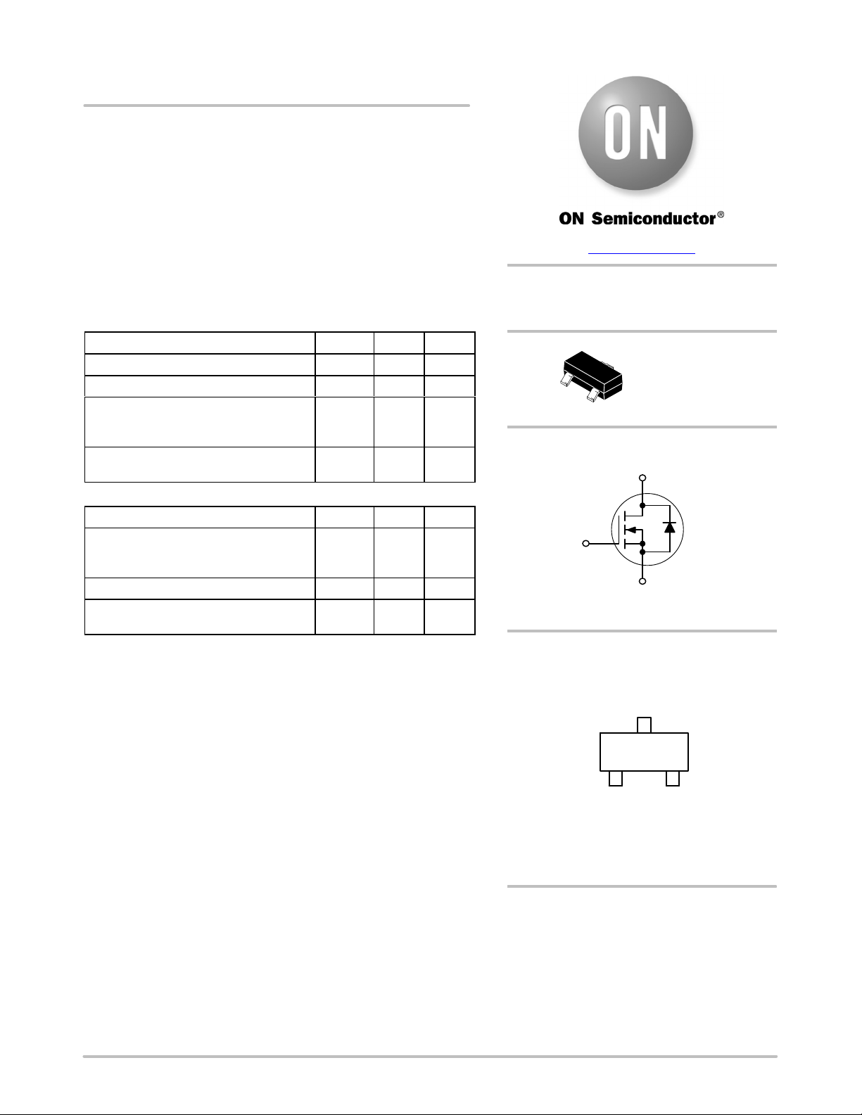
1
2
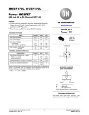
N−Channel
SOT−23
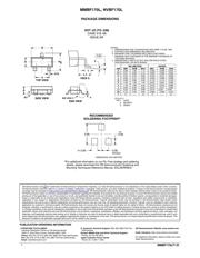
CASE 318
STYLE 21
MARKING DIAGRAM
& PIN ASSIGNMENT
500 mA, 60 V
R
DS(on)
= 5 W
3
Drain
2 SourceGate 1
www.onsemi.com
ORDERING INFORMATION
See detailed ordering and shipping information in the
package dimensions section on page 2 of this data sheet.
6Z MG
G
6Z = Specific Device Code
M = Date Code
G = Pb−Free Package
(Note: Microdot may be in either location)
Verzeichnis
- ・ Konfiguration des Pinbelegungsdiagramms on Seite 1
- ・ Abmessungen des Paketumrisses on Seite 5
- ・ Paket-Footprint-Pad-Layout on Seite 5
- ・ Teilenummerierungssystem on Seite 1 Seite 2 Seite 5
- ・ Markierungsinformationen on Seite 1 Seite 5
- ・ Technische Daten on Seite 2
- ・ Anwendungsbereich on Seite 1
- ・ Elektrische Spezifikation on Seite 2 Seite 3 Seite 4
- ・ Teilenummernliste on Seite 1