
herunterladen
© Semiconductor Components Industries, LLC, 2015
November, 2016− Rev. 14
1 Publication Order Number:
MM5Z2V4T1/D
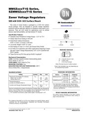
MM5ZxxxT1G Series,
SZMM5ZxxxT1G Series
Zener Voltage Regulators
500 mW SOD−523 Surface Mount
This series of Zener diodes is packaged in a SOD−523 surface
mount package. They are designed to provide voltage regulation
protection and are especially attractive in situations where space is at a
premium. They are well suited for applications such as cellular
phones, hand held portables, and high density PC boards.
Specification Features:
• Standard Zener Breakdown Voltage Range − 2.4 V to 75 V
• Steady State Power Rating of 500 mW
• Small Body Outline Dimensions:
0.047″ x 0.032″ (1.20 mm x 0.80 mm)
• Low Body Height: 0.028″ (0.7 mm)
• ESD Rating of Class 3 (> 16 kV) per Human Body Model
• SZ Prefix for Automotive and Other Applications Requiring Unique
Site and Control Change Requirements; AEC−Q101 Qualified and
PPAP Capable
• These Devices are Pb−Free and are RoHS Compliant*
Mechanical Characteristics:
CASE:
Void-free, transfer-molded, thermosetting plastic
Epoxy Meets UL 94 V−0
LEAD FINISH: 100% Matte Sn (Tin)
MOUNTING POSITION: Any
QUALIFIED MAX REFLOW TEMPERATURE: 260°C
Device Meets MSL 1 Requirements
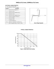
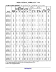
MAXIMUM RATINGS
Rating Symbol Max Unit
Total Device Dissipation FR−4 Board,
(Note 1) @ T
A
= 25°C
Derate above 25°C
P
D
500
4.0
mW
mW/°C
Thermal Resistance,
Junction−to−Ambient (Note 1)
R
q
JA
250 °C/W
Junction and Storage Temperature Range T
J
, T
stg
−65 to
+150
°C
Stresses exceeding those listed in the Maximum Ratings table may damage the
device. If any of these limits are exceeded, device functionality should not be
assumed, damage may occur and reliability may be affected.
1. FR−4 printed circuit board, single−sided copper, mounting pad 1 cm
2
.
*For additional information on our Pb−Free strategy and soldering details, please
download the ON Semiconductor Soldering and Mounting Techniques
Reference Manual, SOLDERRM/D.
Device Package Shipping
†
ORDERING INFORMATION
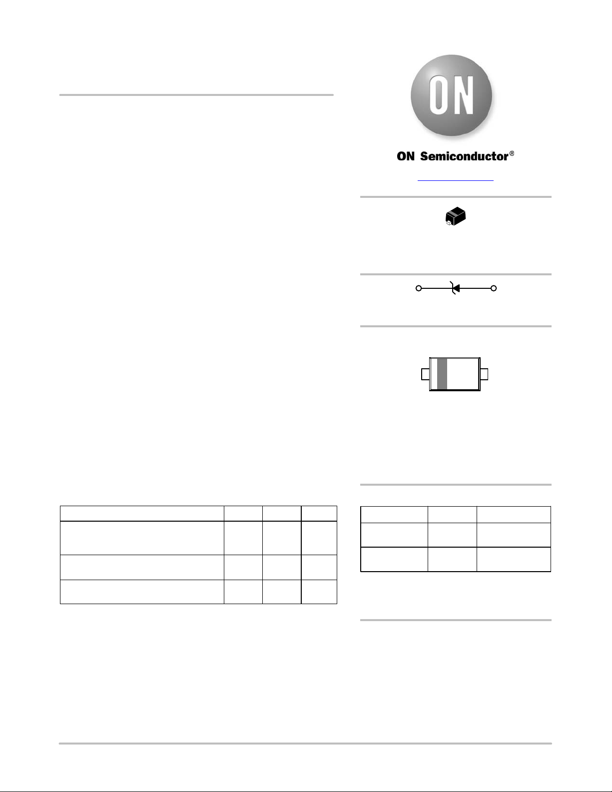
1
Cathode
2
Anode
See specific marking information in the device marking
column of the Electrical Characteristics tables starting on
page 3 of this data sheet.
DEVICE MARKING INFORMATION
www.
onsemi.com
†For information on tape and reel specifications,
including part orientation and tape sizes, please
refer to our Tape and Reel Packaging Specification
s
Brochure, BRD8011/D.
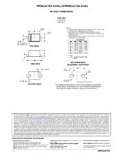
SOD−523
CASE 502
STYLE 1
MARKING DIAGRAM
1
2
MM5ZxxxxT1G SOD−523
(Pb−Free)
3,000 /
Tape & Reel
XX = Specific Device Code
M = Date Code*
G = Pb−Free Package
(Note: Microdot may be in either location)
*Date Code orientation may vary depending up-
on manufacturing location.
XX M G
G
SZMM5ZxxxT1G SOD−523
(Pb−Free)
3,000 /
Tape & Reel
Verzeichnis
- ・ Abmessungen des Paketumrisses on Seite 1 Seite 4
- ・ Paket-Footprint-Pad-Layout on Seite 4
- ・ Teilenummerierungssystem on Seite 1 Seite 4
- ・ Markierungsinformationen on Seite 1 Seite 3 Seite 4
- ・ Technische Daten on Seite 1
- ・ Anwendungsbereich on Seite 1
- ・ Elektrische Spezifikation on Seite 1 Seite 2 Seite 3
- ・ Teilenummernliste on Seite 1