
herunterladen

© 2015 Freescale Semiconductor, Inc. All rights reserved.
Freescale Semiconductor, Inc.
Application Note
Document Number: AN5202
Rev. 1, 10/2015
1 Introduction
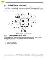
This application note describes Printed Circuit Board
(PCB) design considerations for the MKW40Z and
MKW20Z 48-pin Laminated QFN (LQFN) package as
well as for the MKW30Z 32-pin LQFN package.
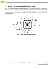
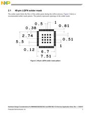
Included are layouts of the component copper layer,
solder mask, and solder paste stencil. These
recommendations are guidelines only and may need to
be modified depending on the assembly house used and
the other components on the board.
Hardware Design Considerations for
MKW40Z/30Z/20Z BLE and IEEE 802.15.4
Devices
Contents
1 Introduction . . . . . . . . . . . . . . . . . . . . . . . . . . . . . . . .1
2 48-pin LQFN component copper layer . . . . . . . . . . .2
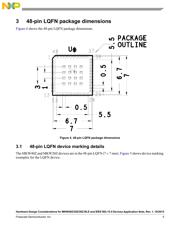
3 48-pin LQFN package dimensions . . . . . . . . . . . . . .5
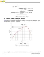
4 48-pin LQFN soldering profile . . . . . . . . . . . . . . . . .6
5 32-pin LQFN component copper layer . . . . . . . . . . .7
6 32-pin LQFN package dimensions . . . . . . . . . . . . .10
7 Design and board layout considerations . . . . . . . . . .11
8 Revision history . . . . . . . . . . . . . . . . . . . . . . . . . . . .17