
herunterladen

© 2016 NXP B.V.
Clock management and distribution in KL28
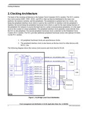
1. Introduction
This application note explains the clock architecture and
clock distribution in KL28. Especially the two new
clock related modules:
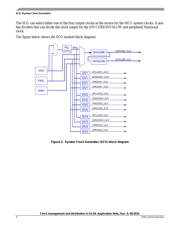
- SCG (System Clock Generator)
- PCC (Peripheral Clock Control)
SCG provides a broad range of reference clocks with
more accuracy than MCG/_Lite, and more flexibility to
work with different applications. With the help of the
SCG, the core clock and peripherals clock can be routed
from different clock sources. This means that the
peripherals clock can be even faster than Core/Bus
clock.
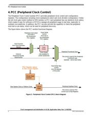
The PCC provides peripheral clock control and
configuration registers, such as clock multiplexors and
clock dividers. Unlike the old clock gate and
configuration in SIM module, the PCC module makes it
easier to select the peripheral clock source and the
software oriented design makes the code more
compatible.
NXP Semiconductors
Document Number: AN5231
Application Note
Rev. 0
,
06/2016
Contents
1. Introduction .................................................................... 1
2. Clocking Architecture...................................................... 2
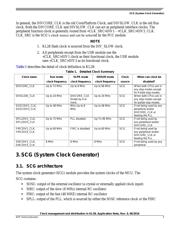
3. SCG (System Clock Generator) ....................................... 3
3.1. SCG architecture................................................... 3
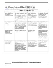
3.2. Difference between SCG and MCG/MCG_Lite ..... 5
4. PCC (Peripheral Clock Control) ....................................... 6
5. SCG Clock Mode Transitions .......................................... 8
5.1. SCG valid clock mode .......................................... 8
5.2. SCG clock mode transitions examples ................ 10
5.3. SCG configuration in HSRUN and VLPR mode .. 12
5.4. Clock configuration in STOP mode ..................... 14
6. References .................................................................... 14
7. Revision History ........................................................... 14