
herunterladen
© Semiconductor Components Industries, LLC, 2013
September, 2013 − Rev. 11
1 Publication Order Number:
MJF6388/D
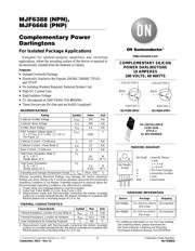
MJF6388 (NPN),
MJF6668 (PNP)
Complementary Power
Darlingtons
For Isolated Package Applications
Designed for general−purpose amplifiers and switching
applications, where the mounting surface of the device is required to
be electrically isolated from the heatsink or chassis.
Features
• Isolated Overmold Package
• Electrically Similar to the Popular 2N6388, 2N6668, TIP102,
and TIP107
• No Isolating Washers Required, Reduced System Cost
• High DC Current Gain
• High Isolation Voltage
• UL Recognized at 3500 VRMS: File #E69369
• These Devices are Pb−Free and are RoHS Compliant*
MAXIMUM RATINGS
Rating Symbol Value Unit
Collector−Emitter Voltage V
CEO
100 Vdc
Collector−Base Voltage V
CB
100 Vdc
Emitter−Base Voltage V
EB
5.0 Vdc
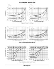
RMS Isolation Voltage (Note 1)
(t = 0.3 sec, R.H. ≤ 30%, T
A
= 25_C)
Per Figure 14
V
ISOL
4500
V
Collector Current − Continuous I
C
10 Adc
Collector Current − Peak (Note 2) I
CM
15 Adc
Base Current − Continuous I
B
1.0 Adc
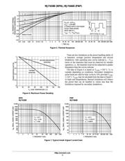
Total Power Dissipation (Note 3)
@ T
C
= 25_C
Derate above 25_C
P
D
40
0.31
W
W/_C
Total Power Dissipation
@ T
A
= 25_C
Derate above 25_C
P
D
2.0
0.016
W
W/_C
Operating and Storage Temperature Range T
J
, T
stg
–65 to +150
_C
Stresses exceeding Maximum Ratings may damage the device. Maximum
Ratings are stress ratings only. Functional operation above the Recommended
Operating Conditions is not implied. Extended exposure to stresses above the
Recommended Operating Conditions may affect device reliability.
1. Proper strike and creepage distance must be provided.
2. Pulse Test: Pulse Width = 5.0 ms, Duty Cycle ≤ 10%.
3. Measurement made with thermocouple contacting the bottom insulated
surface (in a location beneath the die), the devices mounted on a heatsink with
thermal grease and a mounting torque of ≥ 6 in. lbs.
ÎÎÎÎÎÎÎÎÎÎÎÎÎÎÎÎÎÎÎ
ÎÎÎÎÎÎÎÎÎÎÎÎÎÎÎÎÎÎÎ
THERMAL CHARACTERISTICS
ÎÎÎÎÎÎÎÎÎÎÎÎÎ
ÎÎÎÎÎÎÎÎÎÎÎÎÎ
Characteristic
ÎÎÎ
ÎÎÎ
Symbol
ÎÎÎ
ÎÎÎ
Max
ÎÎÎ
ÎÎÎ
Unit
ÎÎÎÎÎÎÎÎÎÎÎÎÎ
ÎÎÎÎÎÎÎÎÎÎÎÎÎ
Thermal Resistance, Junction−to−Case (Note 4)
ÎÎÎ
ÎÎÎ
R
q
JC
ÎÎÎ
ÎÎÎ
4.0
ÎÎÎ
ÎÎÎ
_C/W
ÎÎÎÎÎÎÎÎÎÎÎÎÎ
ÎÎÎÎÎÎÎÎÎÎÎÎÎ
Thermal Resistance, Junction−to−Ambient
ÎÎÎ
ÎÎÎ
R
q
JA
ÎÎÎ
ÎÎÎ
62.5
ÎÎÎ
ÎÎÎ
_C/W
ÎÎÎÎÎÎÎÎÎÎÎÎÎ
Lead Temperature for Soldering Purposes
ÎÎÎ
T
L
ÎÎÎ
260
ÎÎÎ
_C
4. Measurement made with thermocouple contacting the bottom insulated
surface (in a location beneath the die), the devices mounted on a heatsink with
thermal grease and a mounting torque of ≥ 6 in. lbs.
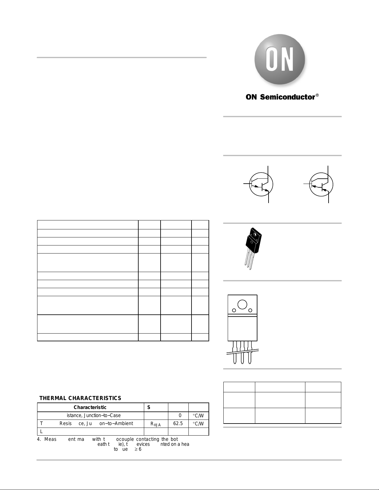
Device Package Shipping
ORDERING INFORMATION
TO−220 FULLPACK
CASE 221D
STYLE 2
UL RECOGNIZED
3
1
COMPLEMENTARY SILICON
POWER DARLINGTONS
10 AMPERES
100 VOLTS, 40 WATTS
2
http://onsemi.com
MJF6668G 50 Units/Rail
MJF6388G TO−220 FULLPACK
(Pb−Free)
50 Units/Rail
MJF6xy8 = Specific Device
Code
x = 3 or 6
y = 6 or 8
G = Pb−Free Package
A = Assembly Location
Y = Year
WW = Work Week
MARKING DIAGRAM
TO−220 FULLPACK
(Pb−Free)
*For additional information on our Pb−Free strategy
and soldering details, please download the
ON Semiconductor Soldering and Mounting
Techniques Reference Manual, SOLDERRM/D.
COLLECTOR 2
BASE
1
EMITTER 3
COLLECTOR 2
BASE
1
EMITTER 3
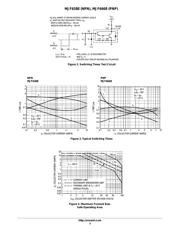
MJF6388 (NPN) MJF6668 (PNP)
MJF6xy8G
AYWW
Verzeichnis